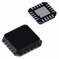
ADF4213BCP Analog Devices Inc, ADF4213BCP Datasheet

ADF4213BCP
Specifications of ADF4213BCP
Available stocks
Related parts for ADF4213BCP
ADF4213BCP Summary of contents
Page 1
IF IN OSCILLATOR REF IN CLOCK 24-BIT DATA DATA REGISTER DGND RF Dual RF/IF PLL Frequency Synthesizers ADF4210/ADF4211/ADF4212/ADF4213 GENERAL DESCRIPTION The ADF4210/ADF4211/ADF4212/ADF4213 is a dual frequency synthesizer that can be used to implement local oscillators (LO) ...
Page 2
ADF4210/ADF4211/ADF4212/ADF4213–SPECIFICATIONS ( 10 10 unless otherwise noted.) A MIN MAX P arameter RF/IF CHARACTERISTICS ( Input Frequency ( ...
Page 3
Parameter POWER SUPPLIES (RF + IF) DD ADF4210 ADF4211 ADF4212 ADF4213 I (RF Only) DD ADF4210 ADF4211 ADF4212 ADF4213 I (IF Only) DD ADF4210 ADF4211 ADF4212 ADF4213 ...
Page 4
... ADF4211BRU –40°C to +85°C ADF4211BCP –40°C to +85°C ADF4212BRU –40°C to +85°C ADF4212BCP –40°C to +85°C ADF4213BRU –40°C to +85°C ADF4213BCP –40°C to +85°C Contact the factory for chip availability 10 10 AGND = DGND = 0 V ...
Page 5
Pin Number TSSOP Mnemonic Function Power Supply for the RF Section. Decoupling capacitors to the ground plane should be placed as DD close as possible to this pin. V the same potential ...
Page 6
ADF4210/ADF4211/ADF4212/ADF4213 –Typical Performance Characteristics FREQUENCY S REAL S IMAG FREQUENCY 11 11 50000000.0 0.955683 –0.052267 2150000000.0 150000000.0 0.956993 –0.112191 2250000000.0 250000000.0 0.935463 –0.185212 2350000000.0 350000000.0 0.919706 –0.252576 2450000000.0 450000000.0 0.871631 –0.323799 2550000000.0 550000000.0 0.838141 –0.350455 2650000000.0 650000000.0 0.799005 –0.408344 2750000000.0 ...
Page 7
REFERENCE –10 LEVEL = –5.7dBm I = 5mA CP PFD FREQUENCY = 200kHz –20 LOOP BANDWIDTH = 35kHz –30 RES. BANDWIDTH = 1kHz VIDEO BANDWIDTH = 1kHz –40 SWEEP = 4.2 SECONDS –50 ...
Page 8
ADF4210/ADF4211/ADF4212/ADF4213 3V REFERENCE – 5mA LEVEL = –17.2dBm CP PFD FREQUENCY = 1MHz –20 LOOP BANDWIDTH = 100kHz –30 RES. BANDWIDTH = 1kHz VIDEO BANDWIDTH = 1kHz –40 SWEEP = 13 SECONDS –50 ...
Page 9
TEMPERATURE – C CIRCUIT DESCRIPTION REFERENCE INPUT SECTION The reference input stage is shown below in Figure 2. SW1 and SW2 are normally-closed switches. SW3 is normally-open. When power-down is ...
Page 10
ADF4210/ADF4211/ADF4212/ADF4213 PHASE FREQUENCY DETECTOR (PFD) AND CHARGE PUMP The PFD takes inputs from the R counter and N counter and produces an output proportional to the phase and frequency difference between them. Figure simplified schematic. The PFD ...
Page 11
IF CP CURRENT SETTING DB23 DB22 DB21 DB20 DB19 DB18 DB17 DB16 DB15 DB14 R15 CP2 CP1 CP0 IF PRESCALER DB23 DB22 DB21 DB20 DB19 DB18 DB17 DB16 DB15 DB14 ...
Page 12
ADF4210/ADF4211/ADF4212/ADF4213 IF CP CURRENT SETTING DB23 DB22 DB21 DB20 DB19 DB18 DB17 DB16 DB15 DB14 CP2 CP1 CP0 CHARGE PUMP OUTPUT 0 NORMAL 1 THREE-STATE P12 P11 FROM RF ...
Page 13
IF PRESCALER DB23 DB22 DB21 DB20 DB19 DB18 DB17 DB16 DB15 DB14 B12 B11 B10 PRESCALER 16/ 32/ 64/ POWER-DOWN 0 ...
Page 14
ADF4210/ADF4211/ADF4212/ADF4213 RF CP CURRENT SETTING DB23 DB22 DB21 DB20 DB19 DB18 DB17 DB16 DB15 DB14 P12 P11 P10 P9 CP2 CP1 CP0 P10 CHARGE PUMP OUTPUT 0 NORMAL 1 THREE-STATE FROM IF R LATCH ...
Page 15
RF PRESCALER DB23 DB22 DB21 DB20 DB19 DB18 DB17 DB16 DB15 DB14 P17 P16 P15 P14 B12 B11 B10 B9 P15 P14 PRESCALER 16/ 32/ 64/65 P16 RF POWER-DOWN 0 DISABLE ...
Page 16
ADF4210/ADF4211/ADF4212/ADF4213 PROGRAM MODES Table III and Table V show how to set up the Program Modes in the ADF421x family. The following should be noted and RF Analog Lock Detect indicate when the PLL is in lock. When ...
Page 17
RF PROGRAM MODES Table III and Table V show how to set up the Program Modes in the ADF421x family. RF Charge Pump Currents RFCP2, RFCP1, RFCP0 program current setting for the RF charge pump. See Table V. PROGRAMMABLE RF ...
Page 18
ADF4210/ADF4211/ADF4212/ADF4213 1000pF 1000pF DD DD FREF REF CLK DATA LE ADF4213 in wide-band applications both of these parameters have a much greater variation. In Figure 8, for example, we have ...
Page 19
PCB Guidelines for Chip Scale Package The lands on the chip scale package (CP-20), are rectangular. The printed circuit board pad for these should be 0.1 mm longer than the package land length and 0.05 mm wider than the package ...
Page 20
ADF4210/ADF4211/ADF4212/ADF4213–Revision History Location Data Sheet changed from REV REV. A. Changes to Test Conditions/Comments section of Specifications . . . . . . . . . . . . . . . . . . . . . ...


