CY7B9945V-5AXCT Cypress Semiconductor Corp, CY7B9945V-5AXCT Datasheet
CY7B9945V-5AXCT
Specifications of CY7B9945V-5AXCT
Available stocks


Related parts for CY7B9945V-5AXCT


CY7B9945V-5AXCT Summary of contents
Page 1
... PRELIMINARY High Speed Multi-phase PLL Clock Buffer Functional Description The CY7B9945V high speed multi-phase PLL clock buffer offers user selectable control over system clock functions. This multiple output clock driver provides the system integrator with functions necessary to optimize the timing of high performance computer and communication systems ...
Page 2
... Absolute Maximum Conditions....................................... 8 Document Number: 38-07336 Rev. *H PRELIMINARY Operating Range............................................................... 8 Electrical Characteristics Over the Operating Range ............................................... 8 Capacitance ...................................................................... 9 Ordering Information...................................................... 11 Package Diagram............................................................ 11 Document History Page ................................................. 12 Sales, Solutions, and Legal Information ...................... 13 Worldwide Sales and Design Support....................... 13 Products .................................................................... 13 PSoC Solutions ......................................................... 13 RoboClock CY7B9945V Page [+] Feedback ...
Page 3
... FBDS[0:1] and FBF0, respectively. See Table 3 and Table 4. LVTTL PLL Lock Indicator. When HIGH, this output indicates that the internal PLL is locked to the reference signal. When LOW, it indicates that the PLL is attempting to acquire lock RoboClock CY7B9945V 39 REFA- 38 REFSEL 37 REFB- 36 REFB+ 35 1F2 ...
Page 4
... The PLL adjusts the phase and the frequency of its output signal to minimize the delay between the reference (REFA/B+, REFA/B-) and the feedback (FB) input signals. The CY7B9945V has a flexible REF input scheme. These inputs enable the use of either differential LVPECL or single ended LVTTL inputs. To configure as single ended LVTTL inputs, leave the complementary pin open (internally pulled to 1 ...
Page 5
... Thus an output programmed with 4tU of skew gets effectively skewed 8t with respect to REF RoboClock CY7B9945V skew. The PLL U matrix shifts with respect to REF. For U [3] Page [+] Feedback ...
Page 6
... HIGH/LOW HIGH LOW MID ) of the V and Phase Generator. f NOM CO when the output connected undivided. NOM RoboClock CY7B9945V 1Q[0:3], 2Q[0:5] LOW ENABLED HIGH HI-Z HIGH HOLD-OFF X FACTORY TEST always appears on an output when the output NOM ). Internal termination resistors hold the ...
Page 7
... MHz is 6. Figure 3. Typical Safe Operating Zone Typical Safe Operating Zone (25-pF Load, 0-m/s air flow) 100 Safe Operating Zone Number of Outputs at 185 MHz RoboClock CY7B9945V Page [+] Feedback ...
Page 8
... IN –400 400 1.0 GND 0.8 [ Max, f – CC MAX V = Max – CC LOAD pF 50 /2, LOAD CC f MAX RoboClock CY7B9945V V CC 3.3V 10 +70 C 3.3V 10% – +85 C Max Unit – V – V 0.5 V 0.5 V A 100 V + 0.3 ...
Page 9
... MHz 3. Description [12, 13] [12, 13] and SKEW0 [14, 15] [16] [5] [5] [11] [19] [19] [20] [12, 21] [21, 22] RoboClock CY7B9945V Min Max Unit – CY7B9945V-2 CY7B9945V-5 Unit Min Max Min Max 24 200 24 200 MHz 24 200 24 200 MHz – 200 – 200 ps – 250 – 250 ps – 250 – ...
Page 10
... LVTTL AC Test Load 2.0V 2.0V 0.8V < (b) TTL Input Test Waveform Figure 5. AC Timing Diagram t SKEWPR t PWL 0.8V t CCJ1-3,4-12 [1:2]Q[0:3] t SKEWBNK [1:2]Q[0: SKEW0,1 Other 185 MHz 200 MHz L RoboClock CY7B9945V [22] 3. 0.8V < [1:2]Q[0,2] t SKEWPR [1:2]Q[1,3] t SKEWBNK t ODCV t ODCV t SKEW0,1 Page [+] Feedback ...
Page 11
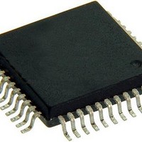
... CY7B9945V-2AXCT 250 200 CY7B9945V-2AXI 200 CY7B9945V-2AXIT 500 200 CY7B9945V-5AXC 200 CY7B9945V-5AXCT Package Diagram Figure 6. 52-Pin Thin Plastic Quad Flat Pack ( 1.4 mm) A52 and AZ52 Document Number: 38-07336 Rev. *H PRELIMINARY Package Package Type Name AZ52 52-pin TQFP AZ52 52-pin TQFP – Tape and Reel ...
Page 12
... Document History Page Document Title: CY7B9945V RoboClock Document Number: 38-07336 Orig. of Submission Revision ECN Change ** 111747 CTK 03/04/02 *A 116572 HWT 09/05/02 *B 119078 HWT 10/16/02 *C 124645 RGL 03/20/03 *D 128464 RGL 07/25/03 *E 272075 RGL See ECN *F 1187144 KVM See ECN *G 2761988 CXQ 09/10/09 ...
Page 13
... RoboClock is a registered trademark, and Total Timing Budget and TTB are trademarks of Cypress Semiconductor. PRELIMINARY cypress.com/go/plc Revised March 12, 2010 2 C components from Cypress or one of its sublicensed Associated Companies conveys a license under the 2 C Standard Specification as defined by Philips.All products and company names RoboClock CY7B9945V PSoC Solutions psoc.cypress.com/solutions PSoC 1 | PSoC 3 | PSoC 5 Page ...