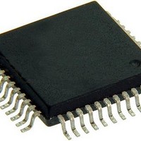
CY7B9945V-5AXCT Cypress Semiconductor Corp, CY7B9945V-5AXCT Datasheet - Page 10

CY7B9945V-5AXCT
Manufacturer Part Number
CY7B9945V-5AXCT
Description
IC CLK BUFF 11OUT 200MHZ 52LQFP
Manufacturer
Cypress Semiconductor Corp
Type
Clock Buffer, Fanout Distributionr
Series
RoboClock™r
Datasheet
1.CY7B9945V-5AXC.pdf
(13 pages)
Specifications of CY7B9945V-5AXCT
Number Of Circuits
1
Package / Case
52-LQFP
Pll
Yes
Input
LVPECL, LVTTL
Output
LVTTL
Ratio - Input:output
4:10
Differential - Input:output
Yes/No
Frequency - Max
200MHz
Divider/multiplier
Yes/Yes
Voltage - Supply
2.97 V ~ 3.63 V
Operating Temperature
0°C ~ 70°C
Mounting Type
Surface Mount
Frequency-max
200MHz
Maximum Input Frequency
200 MHz
Minimum Input Frequency
24 MHz
Output Frequency Range
24 MHz to 200 MHz
Supply Voltage (max)
3.63 V
Supply Voltage (min)
2.97 V
Maximum Operating Temperature
+ 70 C
Minimum Operating Temperature
0 C
Mounting Style
SMD/SMT
Operating Supply Voltage
3.3 V
Lead Free Status / RoHS Status
Lead free / RoHS Compliant
Available stocks
Company
Part Number
Manufacturer
Quantity
Price
Company:
Part Number:
CY7B9945V-5AXCT
Manufacturer:
Cypress Semiconductor Corp
Quantity:
10 000
.
Document Number: 38-07336 Rev. *H
Notes
14. Guaranteed by statistical correlation. Tested initially and after any design or process changes that affects these parameters.
15. Rise and fall times are measured between 2.0V and 0.8V.
16. f
17. t
18. UI = unit interval. Examples: 1 UI is a full period. 0.1UI is 10% of period.
19. Measured at 0.5V deviation from starting voltage.
20. For t
21. These figures are for illustration purposes only. The actual ATE loads may vary.
REF TO DEVICE 1 and 2
FB DEVICE2
FB DEVICE1
NOM
PWH
REF
t
FB
PD
Q
OZA
must be within the frequency range defined by the same FS state.
is measured at 2.0V. t
minimum, C
t
PDELTA
L
= 0 pF. For t
t
t
REFpwh
PD
2.0V
PWL
t
PWH
For LOCK output only
R1 = 910
R2 = 910
C
is measured at 0.8V.
L
OZA
< 30 pF
maximum, C
(Includes fixture and
probe capacitance)
t
REFpwl
t
PDELTA
GND
3.3V
Figure 4. AC Test Loads and Waveforms
< 1 ns
t
L
CCJ1-3,4-12
= 25 pF to 185 MHz or 10 pF to 200 MHz
t
PWL
0.8V
(b) TTL Input Test Waveform
PRELIMINARY
Figure 5. AC Timing Diagram
For all other outputs
R1 = 100
R2 = 100
C
L
< 25 pF to 185 MHz
0.8V
2.0V
or 10 pF at 200 MHz
(a) LVTTL AC Test Load
[1:2]Q[0:3]
[1:2]Q[0:3]
Q
t
Other Q
SKEW0,1
t
t
SKEWBNK
SKEWPR
OUTPUT
2.0V
0.8V
[22]
< 1 ns
C
t
L
ODCV
3.3V
t
ODCV
t
t
SKEW0,1
SKEWBNK
t
SKEWPR
R1
R2
RoboClock
CY7B9945V
[1:2]Q[0,2]
[1:2]Q[1,3]
Page 10 of 13
[+] Feedback


