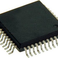
CY7B9945V-5AXCT Cypress Semiconductor Corp, CY7B9945V-5AXCT Datasheet - Page 3

CY7B9945V-5AXCT
Manufacturer Part Number
CY7B9945V-5AXCT
Description
IC CLK BUFF 11OUT 200MHZ 52LQFP
Manufacturer
Cypress Semiconductor Corp
Type
Clock Buffer, Fanout Distributionr
Series
RoboClock™r
Datasheet
1.CY7B9945V-5AXC.pdf
(13 pages)
Specifications of CY7B9945V-5AXCT
Number Of Circuits
1
Package / Case
52-LQFP
Pll
Yes
Input
LVPECL, LVTTL
Output
LVTTL
Ratio - Input:output
4:10
Differential - Input:output
Yes/No
Frequency - Max
200MHz
Divider/multiplier
Yes/Yes
Voltage - Supply
2.97 V ~ 3.63 V
Operating Temperature
0°C ~ 70°C
Mounting Type
Surface Mount
Frequency-max
200MHz
Maximum Input Frequency
200 MHz
Minimum Input Frequency
24 MHz
Output Frequency Range
24 MHz to 200 MHz
Supply Voltage (max)
3.63 V
Supply Voltage (min)
2.97 V
Maximum Operating Temperature
+ 70 C
Minimum Operating Temperature
0 C
Mounting Style
SMD/SMT
Operating Supply Voltage
3.3 V
Lead Free Status / RoHS Status
Lead free / RoHS Compliant
Available stocks
Company
Part Number
Manufacturer
Quantity
Price
Company:
Part Number:
CY7B9945V-5AXCT
Manufacturer:
Cypress Semiconductor Corp
Quantity:
10 000
Pinouts
Pin Definitions
Document Number: 38-07336 Rev. *H
34
40,39, 36,37
38
42
28,18, 35,17, 2, 1 1F[0:3],
19,26
14,12, 13,3
29
50,51
48,46, 32,30,
5,7,8,10, 20,22
44
52
Pin
FS
REFA+,
REFA-
REFB+,
REFB-
REFSEL
FBK
2F[0:1]
DIS[1:2]
[1:2]DS[0:
1]
FBF0
FBDS[0:1]
1Q[0:3],
2Q[0:5]
QF
LOCK
Name
Output
Output
Output
Input
Input
Input
Input
Input
Input
Input
Input
Input
IO
Three level
Three level
Three level
Three level
Three level
VCCN
VCCN
2DS1
1DS1
2DS0
LVDIFF
G ND
G ND
LVTTL/
LVTTL
LVTTL
LVTTL
LVTTL
LVTTL
LVTTL
2Q 0
2Q 1
2Q 2
2Q 3
2F1
2F0
Type
Input
Input
Input
Input
Input
1
2
3
4
5
6
7
8
9
10
11
12
13
PRELIMINARY
52 51 50 49 48 47 46 45 44 43 42 41 40
14 15 16 17 18 19 20 21 22 23 24 25 26
Figure 1. Pin Configuration
Frequency Select. This input must be set according to the nominal frequency
(f
Reference Inputs. These inputs can operate as differential PECL or
single-ended TTL reference inputs to the PLL. When operating as a
single-ended LVTTL input, the complementary input is left open.
Reference Select Input. The REFSEL input controls the configuration of
reference input When LOW, it uses the REFA pair as the reference input. When
HIGH, it uses the REFB pair as the reference input. This input has an internal
pull down.
Feedback Input Clock. The PLL operates such that the rising edges of the
reference and feedback signals are aligned in phase and frequency. This pin
provides the clock output QF feedback to the phase detector.
Output Phase Function Select. Each pair determines the phase of the
respective bank of outputs. See
Output Disable. Each input controls the state of the respective output bank.
When HIGH, the output bank is disabled to HOLD-OFF or High-Z state; the
disable state is determined by MODE. When LOW, outputs 1Q[0:3] and 2Q[0:5]
are enabled. See
Output Divider Function Select. Each pair determines the divider ratio of the
respective bank of outputs. See
Feedback Output Phase Function Select. This input determines the phase
of the QF output. See
Feedback Output Divider Function Select. This input determines the divider
ratio of the QF output. See
Clock Outputs with Adjustable Phases and f
frequencies and phases are determined by [1:2]DS[0:1], and 1F[0:3] and
2F[0:1], respectively. See
Feedback Clock Output. This output is connected to the FBK input. The output
frequency and phase are determined by FBDS[0:1] and FBF0, respectively.
See
PLL Lock Indicator. When HIGH, this output indicates that the internal PLL is
locked to the reference signal. When LOW, it indicates that the PLL is
attempting to acquire lock
NOM
CY7B9945V
Table 3
). See
Table 1.
and
Table
Table
Table
4.
5.
Table 3
Table
3.
39
38
37
36
35
34
33
32
31
30
29
28
27
Table
Table
Description
4.
and
REFA-
REFSEL
REFB-
REFB+
1F2
FS
G ND
1Q 2
VCCN
1Q 3
FBF0
1F0
VCCQ
Table
3.
4.
4.
NOM
Divide Ratios. The output
RoboClock
CY7B9945V
Page 3 of 13
[+] Feedback


