CS5526-BSZ Cirrus Logic Inc, CS5526-BSZ Datasheet - Page 5
CS5526-BSZ
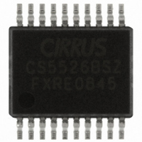
Manufacturer Part Number
CS5526-BSZ
Description
IC ADC 20BIT W/4BIT LATCH 20SSOP
Manufacturer
Cirrus Logic Inc
Datasheet
1.CS5526-BSZ.pdf
(30 pages)
Specifications of CS5526-BSZ
Number Of Converters
1
Package / Case
20-SSOP
Number Of Bits
20
Data Interface
Serial
Power Dissipation (max)
12.7mW
Voltage Supply Source
Analog and Digital
Operating Temperature
-40°C ~ 85°C
Mounting Type
Surface Mount
Number Of Adc Inputs
1
Architecture
Delta-Sigma
Conversion Rate
3.76 SPs to 616 SPs
Resolution
20 bit
Input Type
Voltage
Interface Type
Serial (3-Wire)
Voltage Reference
2.5 V
Supply Voltage (max)
5 V
Supply Voltage (min)
25 mV
Maximum Power Dissipation
500 mW
Maximum Operating Temperature
+ 85 C
Mounting Style
SMD/SMT
Input Voltage
25 mV to 5 V
Minimum Operating Temperature
- 40 C
Lead Free Status / RoHS Status
Lead free / RoHS Compliant
For Use With
598-1014 - EVAL BOARD FOR CS5526
Lead Free Status / Rohs Status
Lead free / RoHS Compliant
Other names
598-1108-5
Available stocks
Company
Part Number
Manufacturer
Quantity
Price
Company:

Part Number:
CS5526-BSZ
Manufacturer:
CIRRUS
Quantity:
1 000
Part Number:
CS5526-BSZ
Manufacturer:
CIRRUS
Quantity:
20 000


DYNAMIC CHARACTERISTICS
RECOMMENDED OPERATING CONDITIONS
Notes: 14. All voltages with respect to ground.
ABSOLUTE MAXIMUM RATINGS
Notes: 15. No pin should go more negative than NBV - 0.3 V.
WARNING: Operation at or beyond these limits may result in permanent damage to the device.
DS202F5
Modulator Sampling Frequency
Filter Settling Time to 1/2 LSB (Full Scale Step)
DC Power Supplies
Analog Reference Voltage
Negative Bias Voltage
DC Power Supplies
Negative Bias Voltage
Input Current, Any Pin Except Supplies
Output Current
Power Dissipation
Analog Input Voltage
Digital Input Voltage
Ambient Operating Temperature
Storage Temperature
16. Applies to all pins including continuous overvoltage conditions at the analog input (AIN) pins.
17. Transient current of up to 100 mA will not cause SCR latch-up. Maximum input current for a power
18. Total power dissipation, including all input currents and output currents.
supply pin is ±50 mA.
Normal operation is not guaranteed at these extremes.
Parameter
Parameter
Parameter
(VREF+) - (VREF-)
Negative Potential
(Note 16 and 17)
Positive Analog
Positive Analog
Positive Digital
Positive Digital
(AGND, DGND = 0 V; See Note 14.)
VREF pins
(Note 15)
(Note 18)
AIN Pins
Symbol
Symbol
Symbol
VRef
NBV
NBV
PDN
V
V
VD+
VD+
I
V
VA+
VA+
T
OUT
I
T
(AGND, DGND = 0 V; See Note 14.))
INR
IND
f
t
INA
IN
stg
s
s
A
diff
4.75
NBV - 0.3
Min
-1.8
2.7
1.0
+0.3
Min
-0.3
-0.3
-0.3
-0.3
-40
-65
-
-
-
CS5525 CS5526
Ratio
XIN/2
1/f
Typ
-2.1
5.0
5.0
2.5
out
(VD+) + 0.3
(VA+) + 0.3
(VA+) + 0.3
Max
+6.0
+6.0
-3.0
±10
±25
500
150
85
Max
5.25
5.25
-2.5
3.0
Unit
Unit
Unit
mW
mA
mA
Hz
°C
°C
V
V
V
V
V
V
V
V
V
V
s
5
Related parts for CS5526-BSZ
Image
Part Number
Description
Manufacturer
Datasheet
Request
R

Part Number:
Description:
IC 20-Bit Delta Sigma Multi-Range ADC
Manufacturer:
Cirrus Logic Inc
Datasheet:

Part Number:
Description:
Development Kit
Manufacturer:
Cirrus Logic Inc
Datasheet:
Part Number:
Description:
Development Kit
Manufacturer:
Cirrus Logic Inc
Datasheet:


Part Number:
Description:
High-efficiency PFC + Fluorescent Lamp Driver Reference Design
Manufacturer:
Cirrus Logic Inc
Datasheet:
Part Number:
Description:
Development Kit
Manufacturer:
Cirrus Logic Inc
Datasheet:
Part Number:
Description:
Development Kit
Manufacturer:
Cirrus Logic Inc
Datasheet:

Part Number:
Description:
Development Kit
Manufacturer:
Cirrus Logic Inc
Datasheet:
Part Number:
Description:
Development Kit
Manufacturer:
Cirrus Logic Inc
Datasheet:
Part Number:
Description:
Development Kit
Manufacturer:
Cirrus Logic Inc
Datasheet:
Part Number:
Description:
Development Kit
Manufacturer:
Cirrus Logic Inc
Datasheet:

Part Number:
Description:
Ref Bd For Speakerbar MSA & DSP Products
Manufacturer:
Cirrus Logic Inc