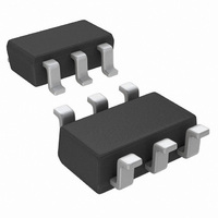
ADCS7477AIMF/NOPB National Semiconductor, ADCS7477AIMF/NOPB Datasheet - Page 19

ADCS7477AIMF/NOPB
Manufacturer Part Number
ADCS7477AIMF/NOPB
Description
IC ADC 10BIT 1MSPS SOT-23-6
Manufacturer
National Semiconductor
Series
PowerWise®r
Datasheet
1.ADCS7478AIMFNOPB.pdf
(24 pages)
Specifications of ADCS7477AIMF/NOPB
Number Of Bits
10
Sampling Rate (per Second)
1M
Data Interface
MICROWIRE™, QSPI™, Serial, SPI™
Number Of Converters
1
Power Dissipation (max)
17.5mW
Voltage Supply Source
Single Supply
Operating Temperature
-40°C ~ 85°C
Mounting Type
Surface Mount
Package / Case
SOT-23-6
Lead Free Status / RoHS Status
Lead free / RoHS Compliant
Other names
ADCS7477AIMF
ADCS7477AIMFTR
ADCS7477AIMFTR
Available stocks
Company
Part Number
Manufacturer
Quantity
Price
Part Number:
ADCS7477AIMF/NOPB
Manufacturer:
TI/德州仪器
Quantity:
20 000
4.0 TYPICAL APPLICATION CIRCUIT
A typical application of the ADCS7476/77/78 is shown in
Figure
vided in this example by the National LP2950 low-dropout
voltage regulator, available in a variety of fixed and adjustable
output voltages. The supply is bypassed with a capacitor net-
work located close to the device. The three-wire interface is
also shown connected to a microprocessor or DSP.
5.0 ANALOG INPUTS
An equivalent circuit for the ADCS7476/77/78 input channel
is shown in
protection for the analog inputs. At no time should an analog
input exceed V
diodes will begin conducting current into the substrate or sup-
ply line and affect ADC operation.
The capacitor C1 in
is mainly due to pin capacitance. The resistor R1 represents
the on resistance of the multiplexer and track / hold switch,
and is typically 100 ohms. The capacitor C2 is the
ADCS7476/77/78 sampling capacitor, and is typically 26 pF.
The sampling nature of the analog input causes input current
pulses that result in voltage spikes at the input. The
ADCS7476/77/78 will deliver best performance when driven
by a low-impedance source to eliminate distortion caused by
the charging of the sampling capacitance. In applications
where dynamic performance is critical, the input might need
to be driven with a low output-impedance amplifier. In addi-
tion, when using the ADCS7476/77/78 to sample AC signals,
a band-pass or low-pass filter will reduce harmonics and
noise and thus improve THD and SNR.
8. The combined analog and digital supplies are pro-
FIGURE 8. Typical Application Circuit
FIGURE 9. Equivalent Input Circuit
Figure
DD
+ 300 mV or GND - 300 mV, as these ESD
Figure 9
9. The diodes D1 and D2 provide ESD
typically has a value of 4 pF, and
20057714
20057713
19
6.0 DIGITAL INPUTS AND OUTPUTS
The ADCS7476/77/78 digital inputs (SCLK and CS) are not
limited by the same absolute maximum ratings as the analog
inputs. The digital input pins are instead limited to +6.5V with
respect to GND, regardless of V
allows the ADCS7476/77/78 to be interfaced with a wide
range of logic levels, independent of the supply voltage.
Note that, even though the digital inputs are tolerant of up to
+6.5V above GND, the digital outputs are only capable of
driving V
to latch-up; SCLK and CS may be asserted before V
out any risk.
7.0 MODES OF OPERATION
The ADCS7476/77/78 has two possible modes of operation:
normal mode, and shutdown mode. The ADCS7476/77/78
enters normal mode (and a conversion process is begun)
when CS is pulled low. The device will enter shutdown mode
if CS is pulled high before the tenth falling edge of SCLK after
CS is pulled low, or will stay in normal mode if CS remains
low. Once in shutdown mode, the device will stay there until
CS is brought low again. By varying the ratio of time spent in
the normal and shutdown modes, a system may trade-off
throughput for power consumption.
8.0 NORMAL MODE
The best possible throughput is obtained by leaving the
ADCS7476/77/78 in normal mode at all times, so there are no
power-up delays. To keep the device in normal mode contin-
uously, CS must be kept low until after the 10th falling edge
of SCLK after the start of a conversion (remember that a con-
version is initiated by bringing CS low).
If CS is brought high after the 10th falling edge, but before the
16th falling edge, the device will remain in normal mode, but
the current conversion will be aborted, and SDATA will return
to TRI-STATE (truncating the output word).
Sixteen SCLK cycles are required to read all of a conversion
word from the device. After sixteen SCLK cycles have
elapsed, CS may be idled either high or low until the next
conversion. If CS is idled low, it must be brought high again
before the start of the next conversion, which begins when
CS is again brought low.
After sixteen SCLK cycles, SDATA returns to TRI-STATE.
Another conversion may be started, after t
by bringing CS low again.
9.0 SHUTDOWN MODE
Shutdown mode is appropriate for applications that either do
not sample continuously, or are willing to trade throughput for
power consumption. When the ADCS7476/77/78 is in shut-
down mode, all of the analog circuitry is turned off.
To enter shutdown mode, a conversion must be interrupted
by bringing CS back high anytime between the second and
tenth falling edges of SCLK, as shown in
CS has been brought high in this manner, the device will enter
shutdown mode; the current conversion will be aborted and
SDATA will enter TRI-STATE. If CS is brought high before the
second falling edge of SCLK, the device will not change
mode; this is to avoid accidentally changing mode as a result
of noise on the CS line.
DD
out. In addition, the digital input pins are not prone
DD
, the supply voltage. This
QUIET
Figure
has elapsed,
www.national.com
10. Once
DD
with-


