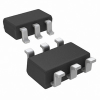
ADCS7477AIMF/NOPB National Semiconductor, ADCS7477AIMF/NOPB Datasheet - Page 9

ADCS7477AIMF/NOPB
Manufacturer Part Number
ADCS7477AIMF/NOPB
Description
IC ADC 10BIT 1MSPS SOT-23-6
Manufacturer
National Semiconductor
Series
PowerWise®r
Datasheet
1.ADCS7478AIMFNOPB.pdf
(24 pages)
Specifications of ADCS7477AIMF/NOPB
Number Of Bits
10
Sampling Rate (per Second)
1M
Data Interface
MICROWIRE™, QSPI™, Serial, SPI™
Number Of Converters
1
Power Dissipation (max)
17.5mW
Voltage Supply Source
Single Supply
Operating Temperature
-40°C ~ 85°C
Mounting Type
Surface Mount
Package / Case
SOT-23-6
Lead Free Status / RoHS Status
Lead free / RoHS Compliant
Other names
ADCS7477AIMF
ADCS7477AIMFTR
ADCS7477AIMFTR
Available stocks
Company
Part Number
Manufacturer
Quantity
Price
Part Number:
ADCS7477AIMF/NOPB
Manufacturer:
TI/德州仪器
Quantity:
20 000
t
t
POWER-UP
Symbol
CONVERT
Timing Test Circuit
ADCS7476/ADCS7477/ADCS7478 Timing Specifications
The following specifications apply for V
other limits T
t
Note 5: Minimum Quiet Time Required Between Bus Relinquish and Start of Next Conversion
Note 6: Measured with the load circuit shown above, and defined as the time taken by the output to cross 1.0V.
Note 7: Measured with the load circuit shown above, and defined as the time taken by the output to cross 1.0V or 2.0V.
Note 8: t
the effects of charging or discharging the 25pF capacitor. This means t
Note 9: All input signals are specified as t
QUIET
t
t
t
t
t
t
t
t
1
2
3
4
5
6
7
8
8
is derived from the time taken by the outputs to change by 0.5V with the loading circuit shown above. The measured number is then adjusted to remove
(Note
Minimum CS Pulse Width
CS to SCLK Setup Time
Delay from CS Until SDATA TRI-STATE
Disabled
Data Access Time after SCLK Falling
Edge(Note
SCLK Low Pulse Width
SCLK High Pulse Width
SCLK to Data Valid Hold Time
SCLK Falling Edge to SDATA High
Impedance
Power-Up Time from Full Power-Down
A
= 25°C, unless otherwise noted.
5)
(Note
7)
(Note
Parameter
6)
8)
r
= t
f
= 5 ns (10% to 90% V
DD
= +2.7V to 5.25V, f
(Note
V
V
V
V
V
V
DD
DD
DD
DD
DD
DD
9)
= +2.7 to +3.6
= +4.75 to +5.25
= +2.7 to +3.6
= +4.75 to +5.25
= +2.7 to +3.6
= +4.75 to +5.25
DD
8
) and timed from 1.6V.
is the true bus relinquish time, independent of the bus loading.
SCLK
9
Conditions
= 20 MHz, Boldface limits apply for T
20057708
16 x t
Typical
1
SCLK
A
0.4 x t
0.4 x t
= −40°C to +85°C: all
Limits
50
10
10
20
40
20
25
25
7
5
6
5
SCLK
SCLK
www.national.com
ns (max)
ns (max)
ns (max)
ns (max)
ns (max)
ns (min)
ns (min)
ns (min)
ns (min)
ns (min)
ns (min)
ns (min)
ns (min)
ns (min)
Units
µs


