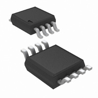
ADC102S101CIMM/NOPB National Semiconductor, ADC102S101CIMM/NOPB Datasheet

ADC102S101CIMM/NOPB
Specifications of ADC102S101CIMM/NOPB
ADC102S101CIMMTR
Available stocks
Related parts for ADC102S101CIMM/NOPB
ADC102S101CIMM/NOPB Summary of contents
Page 1
... ADC082S021 Connection Diagram Ordering Information Order Code ADC102S101CIMM ADC102S101CIMMX ADC102S101EVAL TRI-STATE® trademark of National Semiconductor Corporation QSPI™ and SPI™ are trademarks of Motorola, Inc. © 2010 National Semiconductor Corporation ADC102S101 Features ■ Specified over a range of sample rates. ■ Two input channels ■ ...
Page 2
Block Diagram Pin Descriptions and Equivalent Circuits Pin No. Symbol ANALOG I/O IN1 and IN2 5,4 DIGITAL I/O 8 SCLK 7 DOUT 6 DIN 1 CS POWER SUPPLY GND www.national.com Description Analog inputs. These signals can ...
Page 3
... Absolute Maximum Ratings 2) If Military/Aerospace specified devices are required, please contact the National Semiconductor Sales Office/ Distributors for availability and specifications. Analog Supply Voltage V A Voltage on Any Pin to GND Input Current at Any Pin (Note 3) Package Input Current (Note 3) Power Consumption 25°C ...
Page 4
Symbol Parameter ANALOG INPUT CHARACTERISTICS V Input Range Leakage Current DCL C Input Capacitance INA DIGITAL INPUT CHARACTERISTICS V Input High Voltage IH V Input Low Voltage IL I Input Current IN C Digital Input Capacitance IND ...
Page 5
ADC102S101 Timing Specifications The following specifications apply for 500 ksps to 1 Msps, Boldface limits apply for T SAMPLE Symbol Parameter t Setup Time SCLK High to CS Falling Edge CSU t Hold time SCLK Low to ...
Page 6
Timing Diagrams www.national.com ADC102S101 Operational Timing Diagram Timing Test Circuit ADC102S101 Serial Timing Diagram 6 20125308 20125306 20125351 ...
Page 7
Specification Definitions ACQUISITION TIME is the time required to acquire the input voltage. That is time required for the hold capacitor to charge up to the input voltage. APERTURE DELAY is the time between the fourth falling SCLK ...
Page 8
Typical Performance Characteristics MHz to 16 MHz 40.3 kHz unless otherwise stated. SCLK IN DNL - V = 3.0V A DNL - V = 5.0V A DNL vs. Supply www.national.com T = +25° ...
Page 9
DNL vs. Clock Frequency 20125324 DNL vs. Clock Duty Cycle 20125326 DNL vs. Temperature 20125328 INL vs. Clock Frequency INL vs. Clock Duty Cycle INL vs. Temperature 9 20125325 20125327 20125329 www.national.com ...
Page 10
SNR vs. Supply SNR vs. Clock Frequency SNR vs. Clock Duty Cycle www.national.com THD vs. Supply 20125330 THD vs. Clock Frequency 20125331 THD vs. Clock Duty Cycle 20125332 10 20125335 20125336 20125337 ...
Page 11
SNR vs. Input Frequency 20125333 SNR vs. Temperature 20125334 SFDR vs. Supply 20125340 THD vs. Input Frequency THD vs. Temperature SINAD vs. Supply 11 20125338 20125339 20125345 www.national.com ...
Page 12
SFDR vs. Clock Frequency SFDR vs. Clock Duty Cycle SFDR vs. Input Frequency www.national.com SINAD vs. Clock Frequency 20125341 SINAD vs. Clock Duty Cycle 20125342 SINAD vs. Input Frequency 20125343 12 20125346 20125347 20125348 ...
Page 13
SFDR vs. Temperature 20125344 ENOB vs. Supply 20125352 ENOB vs. Clock Duty Cycle 20125354 SINAD vs. Temperature ENOB vs. Clock Frequency ENOB vs. Input Frequency 13 20125349 20125353 20125355 www.national.com ...
Page 14
ENOB vs. Temperature Spectral Response - 5V, 500 ksps Spectral Response - 5V, 1.0 Msps www.national.com Spectral Response - 3V, 500 ksps 20125356 Spectral Response - 3V, 1.0 Msps 20125365 Power Consumption vs. Throughput 20125360 14 20125364 20125359 20125361 ...
Page 15
Applications Information 1.0 ADC102S101 OPERATION The ADC102S101 is a successive-approximation analog-to- digital converter designed around a charge-redistribution dig- ital-to-analog converter. Simplified schematics of the AD- C102S101 in both track and hold modes are shown in Figures 1, 2, respectively. In ...
Page 16
During each conversion, data is clocked into the ADC at DIN on the first 8 rising edges of SCLK after the fall of CS. For each conversion necessary to clock in the data indicating the input that is ...
Page 17
ADC102S101 TRANSFER FUNCTION The output format of the ADC102S101 is straight binary. Code transitions occur midway between successive integer LSB values. The LSB width for the ADC102S101 is V code of 00 0000 0000 to a code of 00 ...
Page 18
ANALOG INPUTS An equivalent circuit for one of the ADC102S101's input chan- nels is shown in Figure 5. Diodes D1 and D2 provide ESD protection for the analog inputs time should any input go beyond (V + ...
Page 19
Physical Dimensions inches (millimeters) unless otherwise noted Order Number ADC102S101CIMM, ADC102S101CIMMX 8-Lead MSOP NS Package Number P0MUA08A 19 www.national.com ...
Page 20
... For more National Semiconductor product information and proven design tools, visit the following Web sites at: www.national.com Products Amplifiers www.national.com/amplifiers Audio www.national.com/audio Clock and Timing www.national.com/timing Data Converters www.national.com/adc Interface www.national.com/interface LVDS www.national.com/lvds Power Management www.national.com/power Switching Regulators www.national.com/switchers LDOs www.national.com/ldo LED Lighting www ...


