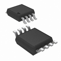
ADC102S101CIMM/NOPB National Semiconductor, ADC102S101CIMM/NOPB Datasheet - Page 18

ADC102S101CIMM/NOPB
Manufacturer Part Number
ADC102S101CIMM/NOPB
Description
IC ADC 10BIT 2CN 1MSPS 8-MSOP
Manufacturer
National Semiconductor
Series
PowerWise®r
Datasheet
1.ADC102S101CIMMNOPB.pdf
(20 pages)
Specifications of ADC102S101CIMM/NOPB
Number Of Bits
10
Sampling Rate (per Second)
1M
Data Interface
DSP, MICROWIRE™, QSPI™, Serial, SPI™
Number Of Converters
1
Power Dissipation (max)
11.4mW
Voltage Supply Source
Single Supply
Operating Temperature
-40°C ~ 85°C
Mounting Type
Surface Mount
Package / Case
8-TSSOP, 8-MSOP (0.118", 3.00mm Width)
For Use With
ADC102S101EVAL - BOARD EVALUATION FOR ADC102S101
Lead Free Status / RoHS Status
Lead free / RoHS Compliant
Other names
ADC102S101CIMM
ADC102S101CIMMTR
ADC102S101CIMMTR
Available stocks
Company
Part Number
Manufacturer
Quantity
Price
Company:
Part Number:
ADC102S101CIMM/NOPB
Manufacturer:
MAXIM
Quantity:
619
www.national.com
5.0 ANALOG INPUTS
An equivalent circuit for one of the ADC102S101's input chan-
nels is shown in
protection for the analog inputs. At no time should any input
go beyond (V
diodes will begin conducting, which could result in erratic op-
eration. For this reason, these ESD diodes should NOT be
used to clamp the input signal.
The capacitor C1 in
is mainly the package pin capacitance. Resistor R1 is the on
resistance of the multiplexer and track / hold switch, and is
typically 500 ohms. Capacitor C2 is the ADC102S101 sam-
pling capacitor and is typically 30 pF. The ADC102S101 will
deliver best performance when driven by a low-impedance
source to eliminate distortion caused by the charging of the
sampling capacitance. This is especially important when us-
ing the ADC102S101 to sample AC signals. Also important
when sampling dynamic signals is a band-pass or low-pass
filter to reduce harmonics and noise, improving dynamic per-
formance.
6.0 DIGITAL INPUTS AND OUTPUTS
The ADC102S101's digital output DOUT is limited by, and
cannot exceed, the supply voltage, V
are not prone to latch-up and, and although not recommend-
ed, SCLK, CS and DIN may be asserted before V
any latchup risk.
7.0 POWER SUPPLY CONSIDERATIONS
The ADC102S101 is fully powered-up whenever CS is low,
and fully powered-down whenever CS is high, with one ex-
ception: the ADC102S101 automatically enters power-down
mode between the 16th falling edge of a conversion and the
1st falling edge of the subsequent conversion (see Timing
Diagrams).
The ADC102S101 can perform multiple conversions back to
back; each conversion requires 16 SCLK cycles. The AD-
C102S101 will perform conversions continuously as long as
CS is held low.
FIGURE 5. Equivalent Input Circuit
A
+ 300 mV) or (GND − 300 mV), as these ESD
Figure
Figure 5
5. Diodes D1 and D2 provide ESD
has a typical value of 3 pF, and
A
. The digital input pins
20125314
A
without
18
The user may trade off throughput for power consumption by
simply performing fewer conversions per unit time. The Power
Consumption vs. Sample Rate curve in the Typical Perfor-
mance Curves section shows the typical power consumption
of the ADC102S101 versus throughput. To calculate the pow-
er consumption, simply multiply the fraction of time spent in
the normal mode by the normal mode power consumption ,
and add the fraction of time spent in shutdown mode multi-
plied by the shutdown mode power dissipation.
7.1 Power Supply Noise Considerations
The charging of any output load capacitance requires current
from the power supply, V
the supply to charge the output capacitance will cause voltage
variations on the supply. If these variations are large enough,
they could degrade SNR and SINAD performance of the ADC.
Furthermore, discharging the output capacitance when the
digital output goes from a logic high to a logic low will dump
current into the die substrate, which is resistive. Load dis-
charge currents will cause "ground bounce" noise in the sub-
strate that will degrade noise performance if that current is
large enough. The larger is the output capacitance, the more
current flows through the die substrate and the greater is the
noise coupled into the analog channel, degrading noise per-
formance.
To keep noise out of the power supply, keep the output load
capacitance as small as practical. If the load capacitance is
greater than 50 pF, use a 100 Ω series resistor at the ADC
output, located as close to the ADC output pin as practical.
This will limit the charge and discharge current of the output
capacitance and improve noise performance.
7.2 Power Supply Noise Considerations
The charging of any output load capacitance requires current
from the power supply, V
the supply to charge the output capacitance will cause voltage
variations on the supply. If these variations are large enough,
they could degrade SNR and SINAD performance of the ADC.
Furthermore, discharging the output capacitance when the
digital output goes from a logic high to a logic low will dump
current into the die substrate, which is resistive. Load dis-
charge currents will cause "ground bounce" noise in the sub-
strate that will degrade noise performance if that current is
large enough. The larger is the output capacitance, the more
current flows through the die substrate and the greater is the
noise coupled into the analog channel, degrading noise per-
formance.
To keep noise out of the power supply, keep the output load
capacitance as small as practical. If the load capacitance is
greater than 50 pF, use a 100 Ω series resistor at the ADC
output, located as close to the ADC output pin as practical.
This will limit the charge and discharge current of the output
capacitance and improve noise performance.
A
A
. The current pulses required from
. The current pulses required from


