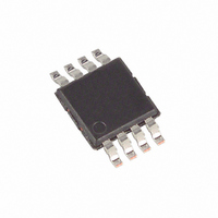
MAX11612EUA+ Maxim Integrated Products, MAX11612EUA+ Datasheet - Page 19

MAX11612EUA+
Manufacturer Part Number
MAX11612EUA+
Description
IC ADC SERIAL 12BIT 4CH 8-MSOP
Manufacturer
Maxim Integrated Products
Datasheet
1.MAX11612EUA.pdf
(22 pages)
Specifications of MAX11612EUA+
Number Of Bits
12
Sampling Rate (per Second)
94.4k
Data Interface
I²C, Serial
Number Of Converters
1
Power Dissipation (max)
362mW
Voltage Supply Source
Single Supply
Operating Temperature
-40°C ~ 85°C
Mounting Type
Surface Mount
Package / Case
8-TSSOP, 8-MSOP (0.118", 3.00mm Width)
Resolution
12 bit
Interface Type
I2C
Snr
70 dB
Voltage Reference
4.096 V
Supply Voltage (max)
5.5 V
Supply Voltage (min)
4.5 V
Maximum Power Dissipation
470.6 mW
Maximum Operating Temperature
+ 85 C
Mounting Style
SMD/SMT
Input Voltage
5 V
Minimum Operating Temperature
- 40 C
For Use With
MAXSPCSPARTAN6+ - ADC and DAC Eval Expansion Board
Lead Free Status / RoHS Status
Lead free / RoHS Compliant
Figure 13. Bipolar Transfer Function
Output data coding for the MAX11612–MAX11617 is
binary in unipolar mode and two’s complement in bipo-
lar mode with 1 LSB = (V
of bits (12). Code transitions occur halfway between
successive-integer LSB values. Figures 12 and 13
show the input/output (I/O) transfer functions for unipo-
lar and bipolar operations, respectively.
Only use PC boards. Wire-wrap configurations are not
recommended since the layout should ensure proper
separation of analog and digital traces. Do not run ana-
log and digital lines parallel to each other, and do not
layout digital signal paths underneath the ADC pack-
age. Use separate analog and digital PCB ground sec-
tions with only one star point (Figure 14) connecting the
two ground systems (analog and digital). For lowest
noise operation, ensure the ground return to the star
ground’s power supply is low impedance and as short
as possible. Route digital signals far away from sensi-
tive analog and reference inputs.
High-frequency noise in the power supply (V
influence the proper operation of the ADC’s fast com-
parator. Bypass V
two parallel capacitors, 0.1µF and 4.7µF, located as
close as possible to the MAX11612–MAX11617 power-
*V
011 . . . 111
011 . . . 110
000 . . . 010
000 . . . 001
000 . . . 000
111 . . . 111
111 . . . 110
111 . . . 101
100 . . . 001
100 . . . 000
COM
≤
OUTPUT CODE
V
REF
Layout, Grounding, and Bypassing
/2
1 LSB =
ZS = 0
-FS =
*V
FS = V
- FS
IN
= (AIN+) - (AIN-)
DD
-V
______________________________________________________________________________________
REF
4096
2
V
2
REF
REF
to the star ground with a network of
REF
INPUT VOLTAGE (LSB)
/2N) where N is the number
Transfer Functions
0
Low-Power, 4-/8-/12-Channel, I
MAX11612–
MAX11617
+FS - 1 LSB
DD
) could
supply pin. Minimize capacitor lead length for best sup-
ply noise rejection, and add an attenuation resistor (5Ω)
in series with the power supply if it is extremely noisy.
Integral nonlinearity (INL) is the deviation of the values on
an actual transfer function from a straight line. This straight
line can be either a best straight-line fit or a line drawn
between the endpoints of the transfer function, once offset
and gain errors have been nullified. The MAX11612–
MAX11617’s INL is measured using the endpoint.
Differential nonlinearity (DNL) is the difference between
an actual step width and the ideal value of 1 LSB. A
DNL error specification of less than 1 LSB guarantees
no missing codes and a monotonic transfer function.
Aperture jitter (t
the time between the samples.
Aperture delay (t
edge of the sampling clock and the instant when an
actual sample is taken.
Figure 14. Power-Supply Grounding Connection
*OPTIONAL
R* = 5Ω
3V OR 5V
V
DD
AJ
) is the sample-to-sample variation in
AD
MAX11612–
MAX11617
0.1μF
4.7μF
) is the time between the falling
SUPPLIES
Differential Nonlinearity
Integral Nonlinearity
GND
V
LOGIC
Aperture Delay
Aperture Jitter
= 3V/5V
Definitions
3V/5V
CIRCUITRY
DIGITAL
DGND
GND
2
C,
19


