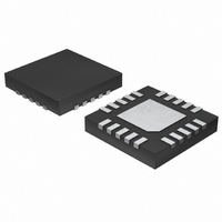
MAX1383ATP+ Maxim Integrated Products, MAX1383ATP+ Datasheet - Page 17

MAX1383ATP+
Manufacturer Part Number
MAX1383ATP+
Description
IC ADC 12BIT 1.25MSPS 20-TQFN
Manufacturer
Maxim Integrated Products
Datasheet
1.MAX1377ATP.pdf
(25 pages)
Specifications of MAX1383ATP+
Number Of Bits
12
Sampling Rate (per Second)
1.25M
Data Interface
DSP, MICROWIRE™, QSPI™, Serial, SPI™
Number Of Converters
2
Power Dissipation (max)
85.5mW
Voltage Supply Source
Single Supply
Operating Temperature
-40°C ~ 85°C
Mounting Type
Surface Mount
Package / Case
20-WQFN, Exposed Pad
Lead Free Status / RoHS Status
Lead free / RoHS Compliant
The internal reference is continuously powered-up dur-
ing both normal and partial power-down modes. In full
power-down mode, the internal reference is disabled.
Allow at least 2ms recovery time after a power-on reset
or exiting full power-down mode for the reference to
settle to its intended value.
The input range on the MAX1383 has an 8x relationship
with the reference voltage. For example, when the refer-
ence voltage (internal or external) is 2.5V, the input
range is ±10V (20V
Drive REFSEL high to select external reference mode.
Apply a reference voltage at REF. Bypass REF with
a 10nF capacitor and a 4.7µF capacitor to RGND. As
with the internal reference, it is important to select a low
ESR capacitor and keep the trace resistance as low
as possible.
Figure 6. Detailed Serial-Interface Timing Diagram
Figure 7. Single-Output CNVST Transition Modes
Dual, 12-Bit, 1.25Msps Simultaneous-Sampling
DOUT_
CNVST
CNVST
SCLK
CS
SCLK
CS
INTERNAL T/H STATE
Input Voltage Range (MAX1383)
t
SETUP
t
CST
______________________________________________________________________________________
P-P
).
External Reference Mode
1
1
t
CL
2
t
CH
3
D11
t
DHOLD
4
D10
POWER-DOWN
ADCs with Serial Interface
D9
HOLD MODE
t
DOUT
D8
14
Upon initial power-up, the MAX1377/MAX1379/ MAX1383
require a complete conversion cycle to initialize the inter-
nal calibration. Following this initialization, the ADC is
ready for normal operation. This initialization is only
required after a hardware power-on reset and is not
required after exiting partial or full power-down mode.
With SCLK idling high or low, a falling edge on CNVST
begins a conversion (see Figure 6). This causes the
analog input stage to transition from track to hold
mode. SCLK provides the timing for the conversion
process, and data is shifted out as each bit of the result
is determined. A rising edge in CNVST forces the
device into one of three modes. The mode is deter-
mined by the clock cycle in which the transition occurs
and whether the device is set for single or dual outputs.
Figures 7 and 8 show each mode that is activated with
a rising CNVST edge for single and dual outputs.
CONTINUOUS MODE
D7
Starting a Conversion and Reading the Output
D6
D5
28
D4
DOUT1 HI-Z
D3
29
Initialization After Power-Up
13
DOUT1 GOES HI-Z
D2
14
D1
Serial Interface
TRACKING
t
ACQ
t
D0
CSW
17


