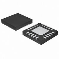
MAX1383ATP+ Maxim Integrated Products, MAX1383ATP+ Datasheet - Page 7

MAX1383ATP+
Manufacturer Part Number
MAX1383ATP+
Description
IC ADC 12BIT 1.25MSPS 20-TQFN
Manufacturer
Maxim Integrated Products
Datasheet
1.MAX1377ATP.pdf
(25 pages)
Specifications of MAX1383ATP+
Number Of Bits
12
Sampling Rate (per Second)
1.25M
Data Interface
DSP, MICROWIRE™, QSPI™, Serial, SPI™
Number Of Converters
2
Power Dissipation (max)
85.5mW
Voltage Supply Source
Single Supply
Operating Temperature
-40°C ~ 85°C
Mounting Type
Surface Mount
Package / Case
20-WQFN, Exposed Pad
Lead Free Status / RoHS Status
Lead free / RoHS Compliant
ELECTRICAL CHARACTERISTICS—MAX1383 (continued)
(V
1µF; T
Minimum Throughput Rate for
Full Bandwidth Signal
Track-and-Hold Acquisition Time
Aperture Delay
Aperture-Delay Matching
Aperture Jitter
External Clock Frequency
ANALOG INPUTS (AIN1A, AIN1B, AIN2A, AIN2B)
Input Range
Differential Input Range
Absolute Voltage Range
Input Impedance
Input Capacitance
EXTERNAL REFERENCE (REFSEL = 1)
Absolute Input Voltage Range
Input Capacitance
Input Current
INTERNAL REFERENCE (REFSEL = 0)
Reference Voltage Level
Load Regulation
Voltage Temperature Coefficient
DIGITAL INPUTS (SCLK, CNVST, U/B, S/D, SEL, REFSEL)
Input-Voltage Low
Input-Voltage High
Input Leakage Current
DIGITAL OUTPUTS (DOUT1, DOUT2)
Output Load Capacitance
Output-Voltage Low
Output-Voltage High
Output Leakage Current
POWER REQUIREMENTS
Analog Supply Voltage
Digital Supply Voltage
Analog Supply Current
Average Static Supply Current
Digital Supply Current
Power-Supply Rejection
AVDD
Dual, 12-Bit, 1.25Msps Simultaneous-Sampling
A
= 4.75V to 5.25V, V
= T
PARAMETER
MIN
to T
MAX
_______________________________________________________________________________________
, unless otherwise noted. Typical values are at T
L
= 1.8V to AVDD, f
SYMBOL
C
f
AVDD
I
V
t
SCLK
AVDD
V
PSR
ACQ
V
DOUT
V
V
I
REF
I
V
I
OL
OH
VL
OL
IL
IH
IL
L
SCLK
(Note 4)
(Note 5)
U/B = 0, V
U/B = 1, V
At each analog input
Time averaged at maximum throughput rate
I
I
For stated timing performance
I
I
High-impedance mode (Figure 9)
Normal operation
Full power-down mode (Note 5)
f
V
SOURCE
SINK
SINK
SOURCE
SCLK
AVDD
= 20MHz (50% duty cycle), V
= 0 to 50µA
= 5mA
= 20MHz, V
= 5V ±10%, full-scale input
= 0 to 1mA
= 1mA, V
ADCs with Serial Interface
AIN
AIN
_
_
A
A
CONDITIONS
- RGND
- V
L
L
AIN
= 3V, C
≥ 2.7V
A
_
= +25°C.)
B
L
= 30pF
REF
= 2.50V, REFSEL = V
V
0.7 x V
1.25
2.48
L
MIN
4.75
-10
-10
-10
10
1.8
- 0.5V
L
±50.0
1600
TYP
2.50
±0.2
125
30
10
50
5.0
0.5
10
±5
55
44
2
2
1
1
2
L
, S/D = DGND, C
0.3 x V
AVDD
MAX
2.52
+10
+10
+10
5.25
±10
±30
2.5
0.4
3.0
20
30
65
10
58
L
ppm/
mV/mA
UNITS
ksps
MHz
kΩ
pF
pF
µA
mA
mA
mA
mV
ns
ns
ns
ps
µA
pF
µA
µA
REF
V
V
V
V
V
V
V
V
V
V
V
o
C
7
=


