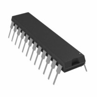
AD7731BNZ Analog Devices Inc, AD7731BNZ Datasheet - Page 12

AD7731BNZ
Manufacturer Part Number
AD7731BNZ
Description
IC ADC 24BIT SIGMA-DELTA 24DIP
Manufacturer
Analog Devices Inc
Datasheet
1.AD7731BRUZ.pdf
(44 pages)
Specifications of AD7731BNZ
Data Interface
DSP, Serial, SPI™
Number Of Bits
24
Sampling Rate (per Second)
6.4k
Number Of Converters
1
Power Dissipation (max)
125mW
Voltage Supply Source
Analog and Digital
Operating Temperature
-40°C ~ 85°C
Mounting Type
Through Hole
Package / Case
24-DIP (0.300", 7.62mm)
Resolution (bits)
24bit
Sampling Rate
6.4kSPS
Input Channel Type
Single Ended
Supply Voltage Range - Analog
4.75V To 5.25V
Supply Voltage Range - Digital
2.7V To 5.25V
Lead Free Status / RoHS Status
Lead free / RoHS Compliant
For Use With
EVAL-AD7731EBZ - BOARD EVALUATION FOR AD7731
Lead Free Status / RoHS Status
Lead free / RoHS Compliant, Lead free / RoHS Compliant
AD7731
Register Name
Communications
Register
Status Register
Data Register
Mode Register
Filter Register
Offset Register
Gain Register
Test Register
H
W
S
S
M
R
I
F
F
E
R
D
D
1
3
N
E
Y
1
2
F
S
S
Z
S
F
F
E
M
R
T
1
2
R
N
D
0
D
O
2
1
Y
S
S
R
F
F
S
M
R
W
T
9
1
N
D
B
1
Write Only
Type
Read Only
Read Only
Read/Write 16 Bits
1
Read/Write 16 Bits
Read/Write 24 Bits
Read/Write 24 Bits
Read/Write 24 Bits
0
Y
S
S
N
R
F
F
R
O
B U
W
8
0
N
/
R
0
0
E
F
S
Z
Z
8 Bits
Size
8 Bits
16 Bits or 24 Bits 000000 Hex
F
E
D
E
M
B
7
R
R
E
S
O
O
N
O
3
S
C
Table V. Summary of On-Chip Registers
F
R
H
C
M
6
D
S
H
P
S
2
1
2
2
S
S
F
K
R
C
M
D
5
S
P I
Power-On/Reset
Default Value
Not Applicable
CX Hex
0174 Hex
2002 Hex
000000 Hex
H
S
1
0
1
1
S
F
F
R
A
–12–
C
M
W
4
S
S
H
S
0
T
L
0
0
Function
All operations to other registers are initiated through
the Communications Register. This controls whether
subsequent operations are read or write operations
and also selects the register for that subsequent opera-
tion. Most subsequent operations return control to
the Communications Register except for the continu-
ous read mode of operation.
Provides status information on conversions, calibra-
tions, settling to step inputs, standby operation and
the validity of the reference voltage.
Provides the most up-to-date conversion result from
the part. Register length can be programmed to be
16 bit or 24 bit.
Controls functions such as mode of operation, uni-
polar/bipolar operation, controlling the function of
AIN3/D1 and AIN4/D0, burnout current and Data
Register word length. It also contains the reference
selection bit, the range selection bits and the channel
selection bits.
Controls the amount of averaging in the first stage
filter, selects the fast step and skip modes and con-
trols the chopping modes on the part.
Contains a 24-bit word which is the offset calibration
coefficient for the part. The contents of this register
are used to provide offset correction on the output
from the digital filter. There are three Offset Regis-
ters on the part and these are associated with input
channel pairs as outlined in Table XIII.
Contains a 24-bit word which is the gain calibration
coefficient for the part. The contents of this register
are used to provide gain correction on the output
from the digital filter. There are three Gain Registers
on the part and these are associated with input chan-
nel pairs as outlined in Table XIII.
Controls the test modes of the part which are used
when testing the part. The user is advised not to
change the contents of this register.
REV. A
REV. 0


