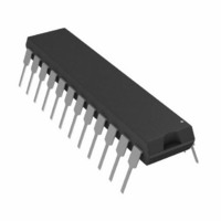
AD7731BNZ Analog Devices Inc, AD7731BNZ Datasheet - Page 14

AD7731BNZ
Manufacturer Part Number
AD7731BNZ
Description
IC ADC 24BIT SIGMA-DELTA 24DIP
Manufacturer
Analog Devices Inc
Datasheet
1.AD7731BRUZ.pdf
(44 pages)
Specifications of AD7731BNZ
Data Interface
DSP, Serial, SPI™
Number Of Bits
24
Sampling Rate (per Second)
6.4k
Number Of Converters
1
Power Dissipation (max)
125mW
Voltage Supply Source
Analog and Digital
Operating Temperature
-40°C ~ 85°C
Mounting Type
Through Hole
Package / Case
24-DIP (0.300", 7.62mm)
Resolution (bits)
24bit
Sampling Rate
6.4kSPS
Input Channel Type
Single Ended
Supply Voltage Range - Analog
4.75V To 5.25V
Supply Voltage Range - Digital
2.7V To 5.25V
Lead Free Status / RoHS Status
Lead free / RoHS Compliant
For Use With
EVAL-AD7731EBZ - BOARD EVALUATION FOR AD7731
Lead Free Status / RoHS Status
Lead free / RoHS Compliant, Lead free / RoHS Compliant
Bit
Location
CR3
CR2-CR0
Status Register (RS2-RS0 = 0, 0, 0); Power-On/Reset Status: CX Hex
The Status Register is an 8-bit read-only register. To access the Status Register, the user must write to the Communications Register
selecting either a single-shot read or continuous read mode and load bits RS2, RS1, RS0 with 0, 0, 0. Table IX outlines the bit desig-
nations for the Status Register. SR0 through SR7 indicate the bit location, SR denoting the bits are in the Status Register. SR7 de-
notes the first bit of the data stream. Figure 5 shows a flowchart for reading from the registers on the AD7731. The number in brackets
indicates the power-on/reset default status of that bit.
Bit
Location
SR7
SR6
SR5
SR4
SR3-SR0
AD7731
R
D
S
Y
R
7
Bit
Mnemonic
ZERO
RS2-RS0
(
Bit
Mnemonic
RDY
STDY
STBY
NOREF
MS3-MS0
) 1
S
T
S
D
R
Y
6
(
) 1
Description
A zero must be written to this bit to ensure correct operation of the AD7731.
Register Selection Bits. RS2 is the MSB of the three selection bits. The three bits select to which
one of eight on-chip registers the next read or write operation takes place as shown in Table VIII.
RS2
0
0
0
0
0
1
1
1
1
Description
Ready Bit. This bit provides the status of the RDY flag from the part. The status and func-
tion of this bit is the same as the RDY output pin. A number of events set the RDY bit high
as indicated in Table XVII.
Steady Bit. This bit is updated when the filter writes a result to the Data Register. If the filter
is in FASTStep™ mode (see Filter Register section), and responding to a step input, the
STDY bit remains high as the initial conversion results become available. The RDY output
and bit are set low on these initial conversions to indicate that a result is available. However,
if the STDY is high, it indicates that the result being provided is not from a fully settled
second-stage FIR filter. When the FIR filter has fully settled, the STDY bit will go low coin-
cident with RDY. If the part is never placed into its FASTStep™ mode, the STDY bit will go
low at the first Data Register read and it is not cleared by subsequent Data Register reads.
A number of events set the STDY bit high as indicated in Table XVII. STDY is set high
along with RDY by all events in the table except a Data Register read.
Standby Bit. This bit indicates whether the AD7731 is in its Standby Mode or normal mode
of operation. The part can be placed in its standby mode using the STANDBY input pin or
by writing 011 to the MD2 to MD0 bits of the Mode Register. The power-on/reset status of
this bit is 0 assuming the STANDBY pin is high.
No Reference Bit. If the voltage between the REF IN(+) and REF IN(–) pins is below 0.5 V
or either of these inputs is open-circuit, the NOREF bit goes to 1. If NOREF is active on
completion of a conversion, the Data Register is loaded with all 1s. If NOREF is active on
completion of a calibration, updating of the calibration registers is inhibited.
These bits are for factory use. The power-on/reset status of these bits varies depending on the
factory-assigned number.
S
T
S
B
R
Y
5
(
) 0
RS1
0
0
0
1
1
0
0
1
1
Table IX. Status Register
N
O
R
S
RS0
0
0
1
0
1
0
1
0
1
R
E
4
F
Table VIII. Register Selection
(
) 0
–14–
Register
Communications Register (Write Operation)
Status Register (Read Operation)
Data Register
Mode Register
Filter Register
No Register Access
Offset Register
Gain Register
Test Register
M
S
S
3
R
3
(
X
)
M
S
S
2
R
2
(
X
)
M
S
S
1
R
1
(
X
)
M
S
S
0
R
0
(
X
)
REV. A
REV. 0


