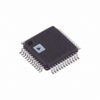
AD7671AST Analog Devices Inc, AD7671AST Datasheet - Page 13

AD7671AST
Manufacturer Part Number
AD7671AST
Description
IC ADC 16BIT CMOS 1MSPS 48-LQFP
Manufacturer
Analog Devices Inc
Series
PulSAR®r
Datasheet
1.AD7671ASTZ.pdf
(24 pages)
Specifications of AD7671AST
Rohs Status
RoHS non-compliant
Number Of Bits
16
Sampling Rate (per Second)
1M
Data Interface
Serial, Parallel
Number Of Converters
1
Power Dissipation (max)
125mW
Voltage Supply Source
Analog and Digital
Operating Temperature
-40°C ~ 85°C
Mounting Type
Surface Mount
Package / Case
48-LQFP
For Use With
EVAL-AD7671CBZ - BOARD EVALUATION FOR AD7671
Available stocks
Company
Part Number
Manufacturer
Quantity
Price
Company:
Part Number:
AD7671ASTZ
Manufacturer:
AD
Quantity:
1 500
Company:
Part Number:
AD7671ASTZ
Manufacturer:
AD
Quantity:
1 045
Company:
Part Number:
AD7671ASTZ
Manufacturer:
Analog Devices Inc
Quantity:
10 000
Part Number:
AD7671ASTZ
Manufacturer:
ADI/亚德诺
Quantity:
20 000
Company:
Part Number:
AD7671ASTZRL
Manufacturer:
Analog Devices Inc
Quantity:
10 000
TYPICAL CONNECTION DIAGRAM
Figure 5 shows a typical connection diagram for the AD7671. Different circuitry shown on this diagram is optional and is discussed below.
REV. B
Description
Full-Scale Range
Least Significant Bit 305.2 mV
FSR – 1 LSB
Midscale + 1 LSB
Midscale
Midscale – 1 LSB
–FSR + 1 LSB
–FSR
NOTES
1
2
3
Values with REF = 2.5 V. With REF = 3 V, all values will scale linearly.
This is also the code for an overrange analog input.
This is also the code for an underrange analog input.
ADR421
2.5V REF
NOTE 1
ANALOG
( 10V)
INPUT
ANALOG
NOTES
1. SEE VOLTAGE REFERENCE INPUT SECTION.
2. WITH THE RECOMMENDED VOLTAGE REFERENCES, C
3. OPTIONAL CIRCUITRY FOR HARDWARE GAIN CALIBRATION.
4. FOR BIPOLAR RANGE ONLY. SEE SCALER REFERENCE INPUT SECTION.
5. THE AD8021 IS RECOMMENDED. SEE DRIVER AMPLIFIER CHOICE SECTION.
6. WITH 0V TO 2.5V RANGE ONLY. SEE ANALOG INPUTS SECTION.
7. OPTION. SEE POWER SUPPLY SECTION.
8. OPTIONAL LOW JITTER CNVST. SEE CONVERSION CONTROL SECTION.
SUPPLY
1
NOTE 5
AD8021
(5V)
100nF
NOTE 3
1M
± 10 V
9.999695 V
305.2 mV
0 V
–305.2 mV
–9.999695 V –4.999847 V –2.499924 V 152.6 mV
–10 V
AD8031
NOTE 4
+
+
U2
U1
50
50k
C
C
+
10 F
NOTE 6
2.7nF
15
Figure 5. Typical Connection Diagram ( ± 10 V Range Shown)
+
+
10 F
± 5 V
152.6 mV
4.999847 V
152.6 mV
0 V
–152.6 mV
–5 V
NOTE 2
100nF
C
REF
Table III. Output Codes and Ideal Input Voltages
100nF
IND
INGND
REF
REFGND
INA
INB
INC
AVDD
± 2.5 V
76.3 mV
2.499924 V
76.3 mV
0 V
–76.3 mV
–2.5 V
NOTE 7
AGND
20
REF
Analog Input
+
IS 47 F. SEE VOLTAGE REFERENCE INPUT SECTION.
10 F
–13–
0 V to 10 V
152.6 mV
9.999847 V 4.999924 V 2.499962 V FFFF
5.000153 V 2.570076 V 1.257038 V 8001
5 V
4.999847 V 2.499924 V 1.249962 V 7FFF
0 V
AD7671
DGND
100nF
DVDD
DVDD
0 V to 5 V
76.3 mV
2.5 V
76.3 mV
0 V
OVDD
BYTESWAP
SER/PAR
IMPULSE
SDOUT
CNVST
OGND
RESET
OB/2C
WARP
BUSY
SCLK
RD
CS
PD
100nF
0 V to 2.5 V
38.15 mV
1.25 V
38.15 mV
0 V
+
50
NOTE 8
DVDD
10 F
Digital Output
Code (Hexa)
Straight Twos
Binary
8000
0001
0000
SERIAL
D
DIGITAL SUPPLY
(3.3V OR 5V)
PORT
CLOCK
3
2
AD7671
Complement
7FFF
0000
8001
8000
0001
FFFF
C/ P/DSP
3
2


