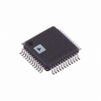
AD7671AST Analog Devices Inc, AD7671AST Datasheet - Page 4

AD7671AST
Manufacturer Part Number
AD7671AST
Description
IC ADC 16BIT CMOS 1MSPS 48-LQFP
Manufacturer
Analog Devices Inc
Series
PulSAR®r
Datasheet
1.AD7671ASTZ.pdf
(24 pages)
Specifications of AD7671AST
Rohs Status
RoHS non-compliant
Number Of Bits
16
Sampling Rate (per Second)
1M
Data Interface
Serial, Parallel
Number Of Converters
1
Power Dissipation (max)
125mW
Voltage Supply Source
Analog and Digital
Operating Temperature
-40°C ~ 85°C
Mounting Type
Surface Mount
Package / Case
48-LQFP
For Use With
EVAL-AD7671CBZ - BOARD EVALUATION FOR AD7671
Available stocks
Company
Part Number
Manufacturer
Quantity
Price
Company:
Part Number:
AD7671ASTZ
Manufacturer:
AD
Quantity:
1 500
Company:
Part Number:
AD7671ASTZ
Manufacturer:
AD
Quantity:
1 045
Company:
Part Number:
AD7671ASTZ
Manufacturer:
Analog Devices Inc
Quantity:
10 000
Part Number:
AD7671ASTZ
Manufacturer:
ADI/亚德诺
Quantity:
20 000
Company:
Part Number:
AD7671ASTZRL
Manufacturer:
Analog Devices Inc
Quantity:
10 000
AD7671
TIMING SPECIFICATIONS
Parameter
Refer to Figures 13, 14, 15, and 16 (Parallel Interface Modes)
Refer to Figures 17 and 18 (Master Serial Interface Modes)
Refer to Figures 19 and 21 (Slave Serial Interface Modes)
NOTES
1
2
3
Specifications subject to change without notice.
DIVSCLK[1]
DIVSCLK[0]
SYNC to SCLK First Edge Delay Minimum
Internal SCLK Period Minimum
Internal SCLK Period Maximum
Internal SCLK HIGH Minimum
Internal SCLK LOW Minimum
SDOUT Valid Setup Time Minimum
SDOUT Valid Hold Time Minimum
SCLK Last Edge to SYNC Delay Minimum
BUSY HIGH Width Maximum (Warp)
BUSY HIGH Width Maximum (Normal)
BUSY HIGH Width Maximum (Impulse)
Specifications subject to change without notice.
In Warp Mode only, the maximum time between conversions is 1 ms; otherwise, there is no required maximum time.
In serial interface modes, the SYNC, SCLK, and SDOUT timings are defined with a maximum load C
In Serial Master Read during Convert Mode. See Table II for Master Read after Convert Mode.
CNVST LOW to DATA Valid Delay
DATA Valid to BUSY LOW Delay
Bus Access Request to DATA Valid
Bus Relinquish Time
CS LOW to SYNC Valid Delay
CS LOW to Internal SCLK Valid Delay
CS LOW to SDOUT Delay
CNVST LOW to SYNC Delay (Read during Convert)
SYNC Asserted to SCLK First Edge Delay
Internal SCLK Period
Internal SCLK HIGH
Internal SCLK LOW
SDOUT Valid Setup Time
SDOUT Valid Hold Time
SCLK Last Edge to SYNC Delay
CS HIGH to SYNC HI-Z
CS HIGH to Internal SCLK HI-Z
CS HIGH to SDOUT HI-Z
BUSY HIGH in Master Serial Read after Convert
CNVST LOW to SYNC Asserted Delay
SYNC Deasserted to BUSY LOW Delay
External SCLK Setup Time
External SCLK Active Edge to SDOUT Delay
SDIN Setup Time
SDIN Hold Time
External SCLK Period
External SCLK HIGH
External SCLK LOW
(Warp Mode/Normal Mode/Impulse Mode)
(Warp Mode/Normal Mode/Impulse Mode)
(Warp Mode/Normal Mode/Impulse Mode)
Master Serial Read after Convert
3
3
3
3
3
Table II. Serial Clock Timings in Master Read after Convert
3
(continued)
3
3
t
t
t
t
t
t
t
t
t
t
t
18
19
19
20
21
22
23
24
28
28
28
2
–4–
0
0
4
25
40
15
9
4.5
2
3
1.5
1.75
2
Symbol
t
t
t
t
t
t
t
t
t
t
t
t
t
t
t
t
t
t
t
t
t
t
t
t
t
t
t
t
10
11
12
13
14
15
16
17
18
19
20
21
22
23
24
25
26
27
28
29
30
31
32
33
34
35
36
37
0
1
20
50
70
25
24
22
4
60
2
2.25
2.5
Min
20
5
4
25
15
9.5
4.5
2
3
5
3
5
5
25
10
10
L
of 10 pF; otherwise, the load is 60 pF maximum.
1
0
20
100
140
50
49
22
30
140
3
3.25
3.5
Typ
25/275/525
See Table II
0.75/1/1.25
25
1
1
20
200
280
100
99
22
89
300
5.25
5.5
5.75
Max
0.75/1/1.25
40
15
10
10
10
40
10
10
10
16
Unit
ns
ns
ns
ns
ns
ns
ns
ns
ms
ms
ms
REV. B
Unit
ms
ns
ns
ns
ns
ns
ns
ns
ns
ns
ns
ns
ns
ns
ns
ns
ns
ms
ms
ns
ns
ns
ns
ns
ns
ns
ns


