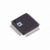
AD7671AST Analog Devices Inc, AD7671AST Datasheet - Page 7

AD7671AST
Manufacturer Part Number
AD7671AST
Description
IC ADC 16BIT CMOS 1MSPS 48-LQFP
Manufacturer
Analog Devices Inc
Series
PulSAR®r
Datasheet
1.AD7671ASTZ.pdf
(24 pages)
Specifications of AD7671AST
Rohs Status
RoHS non-compliant
Number Of Bits
16
Sampling Rate (per Second)
1M
Data Interface
Serial, Parallel
Number Of Converters
1
Power Dissipation (max)
125mW
Voltage Supply Source
Analog and Digital
Operating Temperature
-40°C ~ 85°C
Mounting Type
Surface Mount
Package / Case
48-LQFP
For Use With
EVAL-AD7671CBZ - BOARD EVALUATION FOR AD7671
Available stocks
Company
Part Number
Manufacturer
Quantity
Price
Company:
Part Number:
AD7671ASTZ
Manufacturer:
AD
Quantity:
1 500
Company:
Part Number:
AD7671ASTZ
Manufacturer:
AD
Quantity:
1 045
Company:
Part Number:
AD7671ASTZ
Manufacturer:
Analog Devices Inc
Quantity:
10 000
Part Number:
AD7671ASTZ
Manufacturer:
ADI/亚德诺
Quantity:
20 000
Company:
Part Number:
AD7671ASTZRL
Manufacturer:
Analog Devices Inc
Quantity:
10 000
Pin
No.
21
22
23
24
25–28
29
30
31
32
33
34
35
36
37
38
39
40, 41,
42, 43
NOTES
AI = Analog Input
DI = Digital Input
DI/O = Bidirectional Digital
DO = Digital Output
P = Power
REV. B
Mnemonic
D[8]
or SDOUT
D[9]
or SCLK
D[10]
or SYNC
D[11]
or RDERROR
D[12:15]
BUSY
DGND
RD
CS
RESET
PD
CNVST
AGND
REF
REFGND
INGND
INA, INB,
INC, IND
Type
DO
DI/O
DO
DO
DO
DO
P
DI
DI
DI
DI
DI
P
AI
AI
P
AI
Description
When SER/PAR is LOW, this output is used as Bit 8 of the Parallel Port Data Output Bus.
When SER/PAR is HIGH, this output, part of the Serial Port, is used as a serial data output
synchronized to SCLK. Conversion results are stored in an on-chip register. The AD7671 provides
the conversion result, MSB first, from its internal shift register. The data format is determined
by the logic level of OB/2C. In Serial Mode, when EXT/INT is LOW, SDOUT is valid on both
edges of SCLK.
In Serial Mode, when EXT/INT is HIGH:
If INVSCLK is LOW, SDOUT is updated on SCLK rising edge and valid on the next falling edge.
If INVSCLK is HIGH, SDOUT is updated on SCLK falling edge and valid on the next rising edge.
When SER/PAR is LOW, this output is used as Bit 9 of the Parallel Port Data Output Bus.
When SER/PAR is HIGH, this pin, part of the Serial Port, is used as a serial data clock input or
output, dependent upon the logic state of the EXT/INT pin. The active edge where the data SDOUT
is updated depends upon the logic state of the INVSCLK pin.
When SER/PAR is LOW, this output is used as Bit 10 of the Parallel Port Data Output Bus.
When SER/PAR is HIGH, this output, part of the Serial Port, is used as a digital output frame
synchronization for use with the internal data clock (EXT/INT = Logic LOW). When a read sequence
is initiated and INVSYNC is LOW, SYNC is driven HIGH and remains HIGH while SDOUT
output is valid. When a read sequence is initiated and INVSYNC is HIGH, SYNC is driven LOW
and remains LOW while SDOUT output is valid.
When SER/PAR is LOW, this output is used as Bit 11 of the Parallel Port Data Output Bus.
When SER/PAR is HIGH and EXT/INT is HIGH, this output, part of the Serial Port, is used as an
incomplete read error flag. In Slave Mode, when a data read is started and not complete when the
following conversion is complete, the current data is lost and RDERROR is pulsed HIGH.
Bit 12 to Bit 15 of the Parallel Port Data Output Bus. When SER/PAR is HIGH, these outputs are in
high impedance.
Busy Output. Transitions HIGH when a conversion is started and remains HIGH until the conversion
is complete and the data is latched into the on-chip shift register. The falling edge of BUSY could
be used as a data-ready clock signal.
Must Be Tied to Digital Ground.
Read Data. When CS and RD are both LOW, the Interface Parallel or Serial Output Bus is enabled.
Chip Select. When CS and RD are both LOW, the Interface Parallel or Serial Output Bus is enabled.
CS is also used to gate the external serial clock.
Reset Input. When set to a logic HIGH, reset the AD7671. Current conversion, if any, is aborted.
If not used, this pin could be tied to DGND.
Power-Down Input. When set to a logic HIGH, power consumption is reduced and conversions are
inhibited after the current one is completed.
Start Conversion. A falling edge on CNVST puts the internal sample-and-hold into the hold state
and initiates a conversion. In Impulse Mode (IMPULSE HIGH and WARP LOW), if CNVST is
held LOW when the acquisition phase (t
hold state and a conversion is immediately started.
Must Be Tied to Analog Ground.
Reference Input Voltage.
Reference Input Analog Ground.
Analog Input Ground.
Analog Inputs. Refer to Table I for input range configuration.
PIN FUNCTION DESCRIPTION (continued)
–7–
8
) is complete, the internal sample-and-hold is put into the
AD7671


