AD2S1200WSTZ Analog Devices Inc, AD2S1200WSTZ Datasheet - Page 12
AD2S1200WSTZ
Manufacturer Part Number
AD2S1200WSTZ
Description
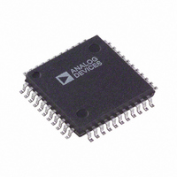
IC R/D CONV W/REF OSCIL 44-LQFP
Manufacturer
Analog Devices Inc
Type
R/D Converterr
Datasheet
1.AD2S1200.pdf
(24 pages)
Specifications of AD2S1200WSTZ
Resolution (bits)
12 b
Data Interface
Serial, Parallel
Voltage Supply Source
Analog and Digital
Voltage - Supply
4.75 V ~ 5.25 V
Operating Temperature
-40°C ~ 125°C
Mounting Type
Surface Mount
Package / Case
44-LQFP
Input Channel Type
Differential
Supply Voltage Range - Analog
4.75V To 5.25V
Supply Voltage Range - Digital
4.75V To 5.25V
Lead Free Status / RoHS Status
Lead free / RoHS Compliant
For Use With
EVAL-AD2S1200CBZ - BOARD EVAL FOR AD2S1200
Sampling Rate (per Second)
-
Lead Free Status / RoHS Status
Lead free / RoHS Compliant, Lead free / RoHS Compliant
Available stocks
Company
Part Number
Manufacturer
Quantity
Price
Company:

Part Number:
AD2S1200WSTZ
Manufacturer:
Analog Devices Inc
Quantity:
135
Company:
Part Number:
AD2S1200WSTZ
Manufacturer:
ADI
Quantity:
276
Company:
Part Number:
AD2S1200WSTZ
Manufacturer:
Analog Devices Inc
Quantity:
10 000


AD2S1200
ABSOLUTE POSITION AND VELOCITY OUTPUT
The angular position and angular velocity are represented by
binary data and can be extracted either via a 12-bit parallel
interface or a 3-wire serial interface that operates at clock rates
up to 25 MHz. The chip select pin, CS , must be held low to
enable the device. Angular position and velocity can be selected
using a dedicated polarity input, RDVEL .
SOE Input
The serial output enable pin, SOE , is held high to enable the
parallel interface. The SOE pin is held low to enable the serial
interface, which places pins (DB0–DB9) in the high impedance
state, while DB11 is the serial output (SO), and DB10 is the
serial clock input (SCLK).
Data Format
The digital angle signal represents the absolute position of the
resolver shaft as a 12-bit unsigned binary word. The digital
velocity signal is a 12-bit twos complement word, which
represents the velocity of the resolver shaft rotating in either a
clockwise or a counterclockwise direction.
Finally, the RD input is used to read the data from the output
register and to enable the output buffer. The timing
requirements for the read cycle are illustrated in Figure 7.
SAMPLE Input
Data is transferred from the position and velocity integrators
respectively to the position and velocity registers following a
high to low transition of the SAMPLE signal. This pin must be
held low for at least t
data. RD should not be pulled low before this time. Also, a
rising edge of SAMPLE resets the internal registers that contain
the minimum and maximum magnitude of the monitor signal.
PARALLEL INTERFACE
The angular position and angular velocity are available on the
AD2S1200 in two 12-bit registers, which can be accessed via the
12-bit parallel port. The parallel interface is selected holding the
SOE pin high. Data is transferred from the velocity and position
1
ns to guarantee correct latching of the
Rev. 0 | Page 12 of 24
integrators, respectively, to the position and velocity registers
following a high-to-low transition on the SAMPLE pin. The
RDVEL polarity pin selects which register from the position or
the velocity registers is transferred to the output register. The CS
pin must be held low to transfer the selected data register to the
output register. Finally, the RD input is used to read the data
from the output register and to enable the output buffer. The
timing requirements for the read cycle are shown in Figure 7.
SAMPLE Input
Data is transferred from the position and velocity integrators,
respectively, to the position and velocity registers following a
high-to-low transition on the SAMPLE signal. This pin must be
held low for at least t
data. RD should not be pulled low before this time since data
would not be ready. The converter will continue to operate
during the read process. Also, a rising edge of SAMPLE resets
the internal registers that contain the minimum and maximum
magnitude of the monitor signal.
CS Input
The device will be enabled when CS is held low.
RDVEL Input
RDVEL input is used to select between the angular position and
velocity registers as shown in Figure 7. RDVEL is held high for
angular position and low for angular velocity. The RDVEL pin
must be set (stable) at least t
RD Input
The 12-bit data bus lines are normally in a high impedance
state. The output buffer is enabled when CS and RD are held
low. A falling edge of the RD signal transfers data to the output
buffer. The selected data is made available to the bus to be read
within t
high impedance state when the RD returns to high state, within
t
reapplied a minimum of t
7
ns. If the user is reading data continuously, RD can be
6
ns of the RD pin going low. The data pins will return to
1
ns to guarantee correct latching of the
5
ns after it was released.
4
ns before the RD pin is pulled low.
Related parts for AD2S1200WSTZ
Image
Part Number
Description
Manufacturer
Datasheet
Request
R

Part Number:
Description:
±1.7g Dual-Axis IMEMS Accelerometer Evaluation Board
Manufacturer:
Analog Devices Inc
Datasheet:

Part Number:
Description:
Inertial Sensor Evaluation System
Manufacturer:
Analog Devices Inc
Datasheet:
Part Number:
Description:
Manufacturer:
Analog Devices Inc
Datasheet:
Part Number:
Description:
Manufacturer:
Analog Devices Inc
Datasheet:
Part Number:
Description:
Manufacturer:
Analog Devices Inc
Datasheet:
Part Number:
Description:
Manufacturer:
Analog Devices Inc
Datasheet:
Part Number:
Description:
Manufacturer:
Analog Devices Inc
Datasheet:
Part Number:
Description:
Manufacturer:
Analog Devices Inc
Datasheet:
Part Number:
Description:
Manufacturer:
Analog Devices Inc
Datasheet:
Part Number:
Description:
Manufacturer:
Analog Devices Inc
Datasheet:
Part Number:
Description:
Manufacturer:
Analog Devices Inc
Datasheet:
Part Number:
Description:
Manufacturer:
Analog Devices Inc
Datasheet:
Part Number:
Description:
Manufacturer:
Analog Devices Inc
Datasheet: