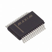
MAX128BCAI+ Maxim Integrated Products, MAX128BCAI+ Datasheet - Page 12

MAX128BCAI+
Manufacturer Part Number
MAX128BCAI+
Description
IC DAS 12BIT 2-WIRE 28-SSOP
Manufacturer
Maxim Integrated Products
Type
Data Acquisition System (DAS)r
Datasheet
1.MAX128BCAI.pdf
(16 pages)
Specifications of MAX128BCAI+
Resolution (bits)
12 b
Sampling Rate (per Second)
8k
Data Interface
Serial
Voltage Supply Source
Single Supply
Voltage - Supply
4.75 V ~ 5.25 V
Operating Temperature
0°C ~ 70°C
Mounting Type
Surface Mount
Package / Case
28-SSOP
Lead Free Status / RoHS Status
Lead free / RoHS Compliant
A conversion cycle begins with the master issuing a
START condition followed by seven address bits
(Figure 3) and a write bit (R/W = 0). Once the eighth bit
has been received and the address matches, the
MAX127/MAX128 (the slave) issues an acknowledge
by pulling SDA low for one clock cycle (A = 0). The
master then writes the input control byte to the slave
(Figure 8). After this byte of data, the slave issues
another acknowledge, pulling SDA low for one clock
cycle. The master ends the write cycle by issuing a
STOP condition (Figure 6).
When the write bit is set (R/W = 0), acquisition starts as
soon as Bit 2 (BIP) of the input control-byte has been
latched and ends when a STOP condition has been
issued. Conversion starts immediately after acquisition.
The MAX127/MAX128’s internal conversion clock fre-
quency is 1.56MHz, resulting in a typical conversion
time of 7.7µs. Figure 9 shows a complete write cycle.
Once a conversion starts, the master does not need to
wait for the conversion to end before attempting to read
the data from the slave. Data access begins with the
master issuing a START condition followed by a 7-bit
address (Figure 3) and a read bit (R/W = 1). Once the
eighth bit has been received and the address matches,
the slave issues an acknowledge by pulling low on SDA
for one clock cycle (A = 0) followed by the first byte of
serial data (D11–D4, MSB first). After the first byte has
been issued by the slave, it releases the bus for the
master to issue an acknowledge (A = 0). After receiv-
ing the acknowledge, the slave issues the second byte
(D3–D0 and four zeros) followed by a NOT acknowl-
edge (A = 1) from the master to indicate that the last
data byte has been received. Finally, the master issues
a STOP condition (P), ending the read cycle (Figure 7).
Multirange, +5V, 12-Bit DAS with
2-Wire Serial Interface
Figure 9. Complete 2-Wire Serial Write Transmission
12
______________________________________________________________________________________
A/D STATE
SDA
SCL
CONDITION
START
Read a Conversion (Read Cycle)
Start a Conversion (Write Cycle)
MSB
0
1
SLAVE ADDRESS BYTE
1
2
7
LSB
W
8
A
9
MSB
10
S
Figure 6. Write Cycle
Figure 7. Read Cycle
Figure 8. Command Byte
START CONDITION
1
S SLAVE ADDRESS R A DATA-BYTE A
SDA
START:
ACK:
SCL
START CONDITION
11
1
S SLAVE ADDRESS W A CONTROL-BYTE A P
CONTROL BYTE
MSB
START SEL2
FIRST LOGIC “1” RECEIVED AFTER ACKNOWLEDGE OF A WRITE.
ACKNOWLEDGE BIT. THE MAX127/MAX128 PULL SDA LOW DURING THE
9TH CLOCK PULSE.
7
BIP
15
7
1 1
READ
16
PD1
ACQUISITION
ACKNOWLEDGE
WRITE
1 1
SEL1 SEL0
ACKNOWLEDGE
PD0
LSB
17
8
A
18
8
1
RNG
CONDITION
DATA-BYTE A P
STOP
NOT ACKNOWLEDGE
ACKNOWLEDGE
8
1 1
BIP
STOP CONDITION
CONVERSION
PD1
1 1
MASTER TO SLAVE
SLAVE TO MASTER
MASTER TO SLAVE
SLAVE TO MASTER
STOP CONDITION
NO. OF BITS
PD0
LSB
NO. OF BITS
ACK


