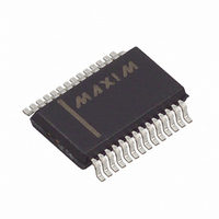
MAX128BCAI+ Maxim Integrated Products, MAX128BCAI+ Datasheet - Page 9

MAX128BCAI+
Manufacturer Part Number
MAX128BCAI+
Description
IC DAS 12BIT 2-WIRE 28-SSOP
Manufacturer
Maxim Integrated Products
Type
Data Acquisition System (DAS)r
Datasheet
1.MAX128BCAI.pdf
(16 pages)
Specifications of MAX128BCAI+
Resolution (bits)
12 b
Sampling Rate (per Second)
8k
Data Interface
Serial
Voltage Supply Source
Single Supply
Voltage - Supply
4.75 V ~ 5.25 V
Operating Temperature
0°C ~ 70°C
Mounting Type
Surface Mount
Package / Case
28-SSOP
Lead Free Status / RoHS Status
Lead free / RoHS Compliant
The MAX127/MAX128 multirange, fault-tolerant ADCs
use successive approximation and internal track/hold
(T/H) circuitry to convert an analog signal to a 12-bit
digital output. Figure 1 shows the block diagram for
these devices.
The T/H circuitry enters its tracking/acquisition mode on
the falling edge of the sixth clock in the 8-bit input con-
trol word and enters its hold/conversion mode when the
master issues a STOP condition. For timing information,
see the
The MAX127/MAX128 have software-selectable input
ranges. Each analog input channel can be indepen-
dently programmed to one of four ranges by setting the
appropriate control bits (RNG, BIP) in the control byte
(Table 1). The MAX127 has selectable input ranges
extending to ±10V (±V
has selectable input ranges extending to ±V
that when an external reference is applied at REFADJ,
the voltage at REF is given by V
(2.4 < V
input circuit.
A resistor network on each analog input provides a
±16.5V fault protection for all channels. This circuit lim-
its the current going into or out of the pin to less than
1.2mA, whether or not the channel is on. This provides
an added layer of protection when momentary over-
voltages occur at the selected input channel, and when
a negative signal is applied at the input even though
Figure 1. Block Diagram
Start a Conversion section.
REF
< 4.18). Figure 2 shows the equivalent
REFADJ
SHDN
CH0
CH1
CH2
CH3
CH4
CH5
CH6
CH7
REF
_______________________________________________________________________________________
Input Range and Protection
Detailed Description
REF
Analog-Input Track/Hold
x 2.441), while the MAX128
Converter Operation
REFERENCE
CONDITIONING
AND SIGNAL
2.5V
REF
ANALOG
INPUT
MUX
= 1.638 x V
Multirange, +5V, 12-Bit DAS with
10k
REF
REFADJ
. Note
1.638
A
V
=
SDA
SERIAL INTERFACE LOGIC
the device may be configured for unipolar mode.
Overvoltage protection is active even if the device is in
power-down mode or V
The MAX127/MAX128 feature a 2-wire serial interface
consisting of the SDA and SCL pins. SDA is the data
I/O and SCL is the serial clock input, controlled by the
master device. A2–A0 are used to program the
MAX127/MAX128 to different slave addresses. (The
MAX127/MAX128 only work as slaves.) The two bus
lines (SDA and SCL) must be high when the bus is not
in use. External pull-up resistors (1k or greater) are
required on SDA and SCL to maintain I
Table 1 shows the input control-byte format.
T/H
Figure 2. Equivalent Input Circuit
2-Wire Serial Interface
S1 = BIPOLAR/UNIPOLAR SWITCH
S2 = INPUT MUX SWITCH
S3, S4 = T/H SWITCH
CH_
A2
R1
A1
IN
REF
A0
5.12k
OUT
S1
S2
R2
12-BIT SAR ADC
HOLD
MAX127
MAX128
DD
SCL
ON
BIPOLAR
UNIPOLAR
R1 = 12.5k (MAX127) OR 5.12k (MAX128)
R2 = 8.67k (MAX127) OR
OFF
= 0.
CLOCK
S3
CLOCK
INT
TRACK
Digital Interface
C
HOLD
TRACK
2
C compatibility.
S4
(MAX128)
VOLTAGE
REFERENCE
T/H
OUT
V
AGND
DGND
HOLD
DD
9


