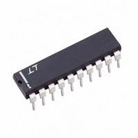
LTC1283ACN#PBF Linear Technology, LTC1283ACN#PBF Datasheet

LTC1283ACN#PBF
Specifications of LTC1283ACN#PBF
Related parts for LTC1283ACN#PBF
LTC1283ACN#PBF Summary of contents
Page 1
... Gain Error (LTC1283A): ±1LSB Max ■ ■ Conversion Time: 44μs ■ Supply Current: 350μA Max, 150μA Typ , LT, LTC and LTM are registered trademarks of Linear Technology Corporation. LTCMOS is a trademark of Linear Technology Corporation. All other trademarks are the property of their respective owners ...
Page 2
LTC1283 BSOLUTE (Notes 1 and 2) Supply Voltage ( GND Voltage Analog and Reference – Inputs ................................. (V Digital Inputs ......................................... –0.3V to 12V Digital Outputs ........................... –0.3V ...
Page 3
VERTER A D ULTIPLEXER CHARACTERISTICS PARAMETER Offset Error Linearity Error Gain Error Minimum Resolution for Which No Missing Codes are Guaranteed Reference Input Resistance Analog and REF Input Range On Channel Leakage Current (Note 7) Off ...
Page 4
LTC1283 U DIGITAL A D ELECTRICAL C DC apply over the full operating temperature range, otherwise specifications are at T SYMBOL PARAMETER I Hi-Z Output Leakage OZ I Output Source Current SOURCE I Output Sink Current SINK I Positive Supply ...
Page 5
W U TYPICAL PERFOR A Change in Full-Scale Error vs Reference Voltage 2 1. 2.5V REF 1.5 1.25 1.0 0.75 0.5 0.25 0 –50 – 100 125 AMBIENT TEMPERATURE (˚C) ...
Page 6
LTC1283 W U TYPICAL PERFOR A Sample-and-Hold Acquisition Time vs Source Resistance 2.5V REF 25° 2.5V INPUT STEP SOURCE 4 + ...
Page 7
TEST CIRCUITS On and Off Channel Leakage Current OFF A POLARITY Load Circuit for dDO r 1. OUT 100pF ACLK CS D OUT WAVEFORM 1 (SEE NOTE 1) ...
Page 8
LTC1283 PPLICATI S I FOR ATIO A The LTC1283 data acquisition component which contains the following functional blocks: 1. 10-bit successive approximation capacitive A/D converter 2. Analog multiplexer (MUX) 3. Sample-and-hold (S&H) 4. Synchronous, ...
Page 9
PPLICATI S I FOR ATIO Multiplexer (MUX) Address The first four bits of the input word assign the MUX configuration for the requested conversion. For a given channel selection, the converter will measure the voltage between ...
Page 10
LTC1283 PPLICATI S I FOR ATIO Unipolar/Bipolar (UNI) The fifth input bit (UNI) determines whether the conver- sion will be unipolar or bipolar. When UNI is a logical one, a unipolar conversion will be performed on ...
Page 11
PPLICATI S I FOR ATIO MSB-First/LSB-First Format (MSBF) The output data of the LTC1283 is programmed for MSB- first or LSB-first sequence using the MSBF bit. For MSB- first output data the input word clocked to ...
Page 12
LTC1283 PPLICATI S I FOR ATIO 8-Bit Word Length CS SCLK 1 (SB) D OUT B9 B8 MSB-FIRST D OUT B0 B1 LSB-FIRST 10-Bit Word Length CS SCLK 1 (SB) D OUT B9 B8 MSB-FIRST D ...
Page 13
PPLICATI S I FOR ATIO SHIFT MUX ADDRESS SAMPLE ANALOG IN CS SCLK SGL/ SEL SEL D DIFF 1 0 ODD/ UNI MSBF WL1 WL0 IN SIGN OUT SHIFT ...
Page 14
LTC1283 PPLICATI S I FOR ATIO Hardware and Software Interface to National Semiconductor COP820C Processor LTC1283 CS SCLK ANALOG • INPUTS • • • D OUT MNEMONIC COMMENTS LD (F0)←0D LOAD 0D INTO F0 ...
Page 15
PPLICATI S I FOR ATIO Texas Instruments TMS70C42 The TMS70C42 transfers serial data in 8-bit increments, LSB-first. To accommodate this, the LTC1283 is pro- grammed for 16-bit word length and LSB-first format. The Hardware and Software ...
Page 16
LTC1283 PPLICATI S I FOR ATIO A MNEMONIC DESCRIPTION MOV P1, #02H INITIALIZE PORT 1 (BIT 1 IS MADE AN INPUT) CLR P1.3 SCLK GOES LOW SETB P1.4 CS GOES LOW CONTINUE: MOV A, #0DH D WORD ...
Page 17
PPLICATI S I FOR ATIO ANALOG GROUND PLANE Figure 6. Example Ground Plane for the ...
Page 18
LTC1283 PPLICATI S I FOR ATIO MUX ADDRESS SHIFTED IN CS SCLK ACLK “+” INPUT “–” INPUT “+” Input Settling This input capacitor is switched onto the “+” input during the sample phase ...
Page 19
PPLICATI S I FOR ATIO HORIZONTAL: 1μs/DIV Figure 12. Poor Op Amp Settling Can Cause A/D Errors RC Input Filtering It is possible to filter the inputs with an RC network as shown in Figure 13. ...
Page 20
LTC1283 PPLICATI S I FOR ATIO differencing operation may not be performed accurately. The conversion time is 44 ACLK cycles. Therefore, a change in the “–” input voltage during this interval can cause conversion errors. For ...
Page 21
PPLICATI S I FOR ATIO when operating at low values of V reduced LSB step size and the resulting higher accuracy requirement placed on the converter. The following factors must be considered when operating at low ...
Page 22
... CH3 IN SNEAK-A-BIT INPUTS D CH4 OUT LTC1283 CS CH5 CH6 REF – – CH7 REF – COM V DGND AGND 0.1μF SNEAK-A-BIT is a trademark of Linear Technology Corp “Quick Look” Circuit for the LTC1283 4.7μF f/ ACLK CLK f SCLK CD4520 OUT REF Q4 – ...
Page 23
... STA $60 STORE MSBs IN $60 Information furnished by Linear Technology Corporation is believed to be accurate and reliable. However, no responsibility is assumed for its use. Linear Technology Corporation makes no represen- tation that the interconnection of its circuits as described herein will not infringe on existing patent rights. S MNEMONIC LOOP 2: ...
Page 24
... MIN .005 .120 .100 (0.127) (3.048) (2.54) MIN MIN BSC : 499-3977 1.060* MAX .065 (1.651) TYP .018 ± .003 (0.457 ± 0.076) N20 0405 LT/CGRAFX 0407 REV B • PRINTED IN USA © LINEAR TECHNOLOGY CORPORATION 1994 1283fb ...


