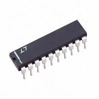
LTC1283ACN#PBF Linear Technology, LTC1283ACN#PBF Datasheet - Page 17

LTC1283ACN#PBF
Manufacturer Part Number
LTC1283ACN#PBF
Description
IC DATA ACQ SYS 10BIT 3V 20-DIP
Manufacturer
Linear Technology
Type
Data Acquisition System (DAS)r
Datasheet
1.LTC1283CN.pdf
(24 pages)
Specifications of LTC1283ACN#PBF
Resolution (bits)
10 b
Sampling Rate (per Second)
15k
Data Interface
Serial, Parallel
Voltage Supply Source
Dual ±
Voltage - Supply
3V
Operating Temperature
0°C ~ 70°C
Mounting Type
Through Hole
Package / Case
20-DIP (0.300", 7.62mm)
Lead Free Status / RoHS Status
Lead free / RoHS Compliant
A
or noise in the output code. V
kept below 1mV by bypassing the V
analog ground plane with a 4.7μF tantalum with leads as
short as possible. Figures 7 and 8 show the effects of good
and poor V
3. Analog Inputs
Because of the capacitive redistribution A/D conversion
techniques used, the analog inputs of the LTC1283 have
capacitive switching input current spikes. These current
spikes settle quickly and do not cause a problem.
However, if large source resistances are used or if slow
settling op amps drive the inputs, care must be taken to
insure that the transients caused by the current spikes
settle completely before the conversion begins.
Source Resistance
The analog inputs of the LTC1283 look like 65pF capacitor
(C
Figure 9. C
“–” inputs once during each conversion cycle. Large
external source resistors and capacitances will slow the
settling of the inputs. It is important that the overall RC
time constants be short enough to allow the analog inputs
to completely settle within the allowed time.
PPLICATI
IN
) in series with a 500Ω resistor (R
Figure 6. Example Ground Plane for the LTC1283
GROUND
ANALOG
PLANE
IN
CC
gets switched between the selected “+” and
bypassing.
O
U
10
1
2
3
4
5
6
7
8
9
S
I FOR ATIO
U
20
19
18
17
16
15
14
13
12
11
CC
noise and ripple can be
V
CC
CC
W
4.7μF
TANTALUM
pin directly to the
ON
) as shown in
0.1µF
CERAMIC
DISK
V
–
U
LTC1283 • F06
V
V
Figure 8. Good V
on V
IN
IN
–
+
Figure 7. Poor V
can Cause A/D Errors
CC
R
R
Figure 9. Analog Input Equivalent Circuit
Below 1mV
SOURCE
SOURCE
+
–
CC
C1
INPUT
INPUT
C2
Bypassing Keeps Noise and Ripple
“+”
“–”
HORIZONTAL: 10μs/DIV
HORIZONTAL: 10μs/DIV
CC
Bypassing. Noise and Ripple
4TH SCLK
LAST SCLK
R
ON
= 500Ω
LTC1283
LTC1283
C
65pF
LTC1283 • F09
IN
=
17
1283fb


