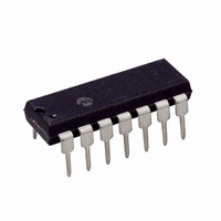
MCP4922-E/P Microchip Technology, MCP4922-E/P Datasheet - Page 20

MCP4922-E/P
Manufacturer Part Number
MCP4922-E/P
Description
IC DAC 12BIT DUAL W/SPI 14DIP
Manufacturer
Microchip Technology
Specifications of MCP4922-E/P
Number Of Converters
2
Package / Case
14-DIP (0.300", 7.62mm)
Settling Time
4.5µs
Number Of Bits
12
Data Interface
Serial, SPI™
Voltage Supply Source
Single Supply
Operating Temperature
-40°C ~ 125°C
Mounting Type
Through Hole
Resolution
12 bit
Interface Type
Serial (3-Wire, SPI, Microwire)
Supply Voltage (max)
5.5 V
Supply Voltage (min)
2.7 V
Maximum Operating Temperature
+ 125 C
Mounting Style
Through Hole
Minimum Operating Temperature
- 40 C
Lead Free Status / RoHS Status
Lead free / RoHS Compliant
Power Dissipation (max)
-
Lead Free Status / Rohs Status
Lead free / RoHS Compliant
Available stocks
Company
Part Number
Manufacturer
Quantity
Price
Company:
Part Number:
MCP4922-E/P
Manufacturer:
MICROCHIP
Quantity:
1 000
Part Number:
MCP4922-E/P
Manufacturer:
MICROCH
Quantity:
20 000
MCP4902/4912/4922
FIGURE 4-2:
4.1.3
An offset error is the deviation from zero voltage output
when the digital input code is zero.
4.1.4
A gain error is the deviation from the ideal output,
V
4.2
4.2.1
The DAC’s outputs are buffered with a low-power,
precision CMOS amplifier. This amplifier provides low
offset voltage and low noise. The output stage enables
the device to operate with output voltages close to the
power supply rails. Refer to Section 1.0 “Electrical
Characteristics” for the analog output voltage range
and load conditions.
In addition to resistive load driving capability, the
amplifier will also drive high capacitive loads without
oscillation. The amplifier’s strong outputs allow V
be used as a programmable voltage reference in a
system.
Selecting a gain of 2 reduces the bandwidth of the
amplifier in Multiplying mode. Refer to Section 1.0
“Electrical Characteristics” for the Multiplying mode
bandwidth for given load conditions.
4.2.1.1
The rail-to-rail output amplifier has configurable gain,
allowing optimal full-scale outputs for different voltage
reference inputs. The output amplifier gain has two
selections, a gain of 1x (<GA> = 1) or a gain of 2x
(<GA> = 0).
The default value is a gain of 2 (<GA> = 0).
DS22250A-page 20
Digital
Input
Code
REF
– 1 LSb, excluding the effects of offset error.
Circuit Descriptions
111
110
101
100
011
010
001
000
OFFSET ERROR
GAIN ERROR
OUTPUT AMPLIFIERS
Programmable Gain Block
Actual
transfer
function
DAC Output
Example for DNL Accuracy.
Narrow code, < 1 LSb
Wide code, > 1 LSb
Ideal transfer
function
OUT
to
4.2.2
The input buffer amplifiers for the MCP4902/4912/4922
devices provide low offset voltage and low noise. A
Configuration bit for each DAC allows the V
bypass the V
Buffered or Unbuffered mode. Buffered mode provides
a very high input impedance, with only minor limitations
on the
Unbuffered (<BUF> = 0) is the default configuration.
Unbuffered mode provides a wide input range (0V to
V
7 pF.
4.2.3
The internal Power-on Reset (POR) circuit monitors the
power supply voltage (V
operation. The circuit also ensures that the DACs
power-up with high output impedance (<SHDN> = 0,
typically 500 k. The devices will continue to have a
high-impedance output until a valid write command is
performed to either of the DAC registers and the LDAC
pin meets the input low threshold.
If the power supply voltage is less than the POR
threshold (V
in their Reset state. The DACs will remain in that state
until V
received.
Figure 4-3
pulse and the duration required to cause a reset to
occur, as well as the relationship between the duration
and trip voltage. A 0.1 µF decoupling capacitor,
mounted as close as possible to the V
provide additional transient immunity.
FIGURE 4-3:
DD
), with a typical input impedance of 165 k with
DD
> V
input
VOLTAGE REFERENCE
AMPLIFIERS
POWER-ON RESET CIRCUIT
shows a typical power supply transient
POR
5V
POR
REF
10
8
6
4
2
0
= 2.0V, typical), the DACs will be held
range
and a subsequent write command is
Transients
input buffer amplifiers, achieving a
1
Typical Transient Response.
2010 Microchip Technology Inc.
V
Transients
Time
DD
and
T
below
A
2
– V
DD
Transient Duration
POR
V
) during the device
DD
frequency
the
3
=
above
(V)
- V
POR
4
the
V
POR
DD
5
REF
response.
pin, can
input to


