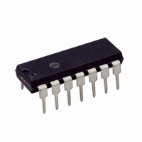
MCP4922-E/P Microchip Technology, MCP4922-E/P Datasheet - Page 28

MCP4922-E/P
Manufacturer Part Number
MCP4922-E/P
Description
IC DAC 12BIT DUAL W/SPI 14DIP
Manufacturer
Microchip Technology
Specifications of MCP4922-E/P
Number Of Converters
2
Package / Case
14-DIP (0.300", 7.62mm)
Settling Time
4.5µs
Number Of Bits
12
Data Interface
Serial, SPI™
Voltage Supply Source
Single Supply
Operating Temperature
-40°C ~ 125°C
Mounting Type
Through Hole
Resolution
12 bit
Interface Type
Serial (3-Wire, SPI, Microwire)
Supply Voltage (max)
5.5 V
Supply Voltage (min)
2.7 V
Maximum Operating Temperature
+ 125 C
Mounting Style
Through Hole
Minimum Operating Temperature
- 40 C
Lead Free Status / RoHS Status
Lead free / RoHS Compliant
Power Dissipation (max)
-
Lead Free Status / Rohs Status
Lead free / RoHS Compliant
Available stocks
Company
Part Number
Manufacturer
Quantity
Price
Company:
Part Number:
MCP4922-E/P
Manufacturer:
MICROCHIP
Quantity:
1 000
Part Number:
MCP4922-E/P
Manufacturer:
MICROCH
Quantity:
20 000
MCP4902/4912/4922
6.4
The MCP4902/4912/4922 family of devices are rail-to-
rail voltage output DAC devices designed to operate
with a V
robust enough to drive small-signal loads directly.
Therefore, it does not require any external output buffer
for most applications.
6.4.1
A common application for the DAC devices is
digitally-controlled set points and/or calibration of
variable parameters, such as sensor offset or slope.
For example, the MCP4922 provides 4096 output
steps. If the external voltage reference (V
4.096V, the LSb size is 1 mV. If a smaller output step
size is desired, a lower external voltage reference is
needed.
EXAMPLE 6-1:
DS22250A-page 28
(b) Dual Output DAC:
(a) Single Output DAC:
DD
Single-Supply Operation
range of 2.7V to 5.5V. Its output amplifier is
DC SET POINT OR CALIBRATION
SPI
V
REF
V OUT
V trip
3-wire
EXAMPLE CIRCUIT OF SET POINT OR THRESHOLD CALIBRATION
MCP4912
MCP4922
MCP4902
MCP4901
MCP4911
MCP4921
=
=
V
V
V OUT
DD
DAC
REF
G
--------------------
R 1
D
------
2
R 2
+
V
N
n
OUT
R 2
REF
R
1
) is
R
D
N = DAC Bit Resolution
G = Gain selection (1x or 2x)
2
n
= Digital value of DAC (0-4095) for MCP4921/MCP4922
= Digital value of DAC (0-255) for MCP4901/MCP4902
= Digital value of DAC (0-1023) for MCP4911/MCP4912
R
SENSE
6.4.1.1
If the application is calibrating the bias voltage of a
diode or transistor, a bias voltage range of 0.8V may be
desired with about 200 µV resolution per step. Two
common methods to achieve a 0.8V range is to either
reduce V
DAC’s output.
Using a V
the
occasionally, when using a low-voltage V
floor causes SNR error that is intolerable. Using a
voltage divider method is another option and provides
some advantages when V
when the desired output voltage is not available. In this
case, a larger value V
scale the output range down to the precise desired
level.
Example 6-1
bypass capacitor on the output of the voltage divider
plays a critical function in attenuating the output noise
of the DAC and the induced noise from the
environment.
V
DD
desired
REF
REF
0.1 uF
Decreasing Output Step Size
to 0.82V or use a voltage divider on the
illustrates this concept. Note that the
is an option if the V
output
V
TRIP
REF
2010 Microchip Technology Inc.
voltage
Comparator
REF
is used while two resistors
needs to be very low or
V
V
CC
CC
REF
+
–
range.
is available with
REF
, the noise
However,
V
O


