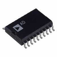
AD7226KRZ Analog Devices Inc, AD7226KRZ Datasheet - Page 10

AD7226KRZ
Manufacturer Part Number
AD7226KRZ
Description
IC DAC 8BIT LC2MOS QUAD 20-SOIC
Manufacturer
Analog Devices Inc
Datasheet
1.AD7226KRZ.pdf
(16 pages)
Specifications of AD7226KRZ
Data Interface
Parallel
Settling Time
4µs
Number Of Bits
8
Number Of Converters
4
Voltage Supply Source
Dual ±
Operating Temperature
-40°C ~ 85°C
Mounting Type
Surface Mount
Package / Case
20-SOIC (7.5mm Width)
Resolution (bits)
8bit
Sampling Rate
143kSPS
Input Channel Type
Parallel
Supply Current
13mA
Digital Ic Case Style
SOIC
No. Of Pins
20
Number Of Channels
4
Resolution
8b
Conversion Rate
143KSPS
Interface Type
Parallel
Single Supply Voltage (typ)
15V
Dual Supply Voltage (typ)
-5/12/-5/15V
Architecture
R-2R
Power Supply Requirement
Single/Dual
Output Type
Voltage
Integral Nonlinearity Error
±0.5LSB
Single Supply Voltage (min)
14.25V
Single Supply Voltage (max)
15.75V
Dual Supply Voltage (min)
-4.5/11.4V
Dual Supply Voltage (max)
-5.5/16.5V
Operating Temp Range
-40C to 85C
Operating Temperature Classification
Industrial
Mounting
Surface Mount
Pin Count
20
Package Type
SOIC W
Lead Free Status / RoHS Status
Lead free / RoHS Compliant
Power Dissipation (max)
-
Lead Free Status / Rohs Status
Compliant
Available stocks
Company
Part Number
Manufacturer
Quantity
Price
Part Number:
AD7226KRZ
Manufacturer:
ADI/亚德诺
Quantity:
20 000
Part Number:
AD7226KRZ-REEL
Manufacturer:
ADI/亚德诺
Quantity:
20 000
Part Number:
AD7226KRZ-REEL7
Manufacturer:
ADI/亚德诺
Quantity:
20 000
AD7226
For a given V
reduce the effective V
ensure specified operation. Note that because the AGND pin is
common to all four DACs, this method biases up the output
voltages of all the DACs in the AD7226. Note that V
of the AD7226 should be referenced to DGND.
3-PHASE SINE WAVE
The circuit of Figure 11 shows an application of the AD7226 in
the generation of 3-phase sine waves which can be used to con-
trol small 3-phase motors. The proper codes for synthesizing a
full sine wave are stored in EPROM, with the required phase-
shift of 120∞ between the three D/A converter outputs being
generated in software.
Data is loaded into the three D/A converters from the sine
EPROM via the microprocessor or control logic. Three loops are
Figure 12. Variation of V
V
BIAS
4.0 V
3.5 V
3.0 V
2.5 V
2.0 V
1.5 V
AGND
V
IN
IN
IN
IN
IN
IN
IN
0 16 32 48 64 80 96 112 128 144 160 176 192 208 224 240 256
R
R
5
IN
F
F
= 2R
= R
, increasing AGND above system GND will
Figure 10. AGND Bias Circuit
R
F
= 3R
DAC A
V
DD
DIGITAL CODE (Decimal Equivalent)
REF
AD7226
–V
REF
REF
* DIGITAL INPUTS OMITTED FOR CLARITY
MICROPROCESSOR
V
CONTROL LOGIC
*
SS
which must be at least 4 V to
with Feedback Configuration
OR
V
Figure 11. 3-Phase Sine Wave Generation Circuit
DGND
DD
V
OUT
V
A
DD
V
SS
= +15 V
DD
EPROM
= –5 V
SINE
ADDRESS
and V
BUS
ADDRESS
DECODE
SS
–10–
DATA
BUS
generated in software with each D/A converter being loaded
from a separate loop. The loops run through the look-up table
producing successive triads of sinusoidal values with 120∞
separation which are loaded to the D/A converters producing
three sine wave voltages 120∞ apart. A complete sine wave
cycle is generated by stepping through the full look-up table.
If a 256-element sine wave table is used then the resolution of
the circuit will be 1.4∞ (360∞/256). Figure 13 shows typical
resulting waveforms. The sine waves can be smoothed by filter-
ing the D/A converter outputs.
The fourth D/A converter of the AD7226, DAC D, may be
used in a feedback configuration to provide a programmable
reference voltage for itself and the other three converters. This
configuration is shown in Figure 11. The relationship of V
V
R and is given by the formula.
where G = R
and D
Alternatively, for a given V
value of D
the expression
Figure 12 shows typical plots of V
three different values of R
peak-to-peak sine wave voltage from the converter outputs will
vary between 2.5 V and 10 V over the digital input code range
of 0 to 255.
IN
is dependent upon digital code and upon the ratio of R
V
D
D
REF
D
is a fractional representation of the digital word in latch D.
WR
A0
A1
=
D
AD7226
=
Figure 13. 3-Phase Sine Wave Output
(
1
for a given value of V
V
F
(
REF
+
1
/R
R R
+
(
1
G
/
+
¥
G
V
V
V
V
F
OUT
OUT
OUT
OUT
D
)
)
¥
D
A
B
C
D
V
)
V
F
V
¥
IN
. With V
IN
REF
IN
V
R
and resistance ratio, the required
IN
R
–
F
REF
R
REF
R
IN
F
can be determined from
versus digital code for
= 2.5 V and R
F
V
V
V
OUT
OUT
OUT
= 3 R the
REV.
B
C
A
REF
F
to
(6)
(7)
to
D


