AD7226KRZ Analog Devices Inc, AD7226KRZ Datasheet - Page 6
AD7226KRZ
Manufacturer Part Number
AD7226KRZ
Description
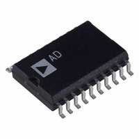
IC DAC 8BIT LC2MOS QUAD 20-SOIC
Manufacturer
Analog Devices Inc
Datasheet
1.AD7226KRZ.pdf
(16 pages)
Specifications of AD7226KRZ
Data Interface
Parallel
Settling Time
4µs
Number Of Bits
8
Number Of Converters
4
Voltage Supply Source
Dual ±
Operating Temperature
-40°C ~ 85°C
Mounting Type
Surface Mount
Package / Case
20-SOIC (7.5mm Width)
Resolution (bits)
8bit
Sampling Rate
143kSPS
Input Channel Type
Parallel
Supply Current
13mA
Digital Ic Case Style
SOIC
No. Of Pins
20
Number Of Channels
4
Resolution
8b
Conversion Rate
143KSPS
Interface Type
Parallel
Single Supply Voltage (typ)
15V
Dual Supply Voltage (typ)
-5/12/-5/15V
Architecture
R-2R
Power Supply Requirement
Single/Dual
Output Type
Voltage
Integral Nonlinearity Error
±0.5LSB
Single Supply Voltage (min)
14.25V
Single Supply Voltage (max)
15.75V
Dual Supply Voltage (min)
-4.5/11.4V
Dual Supply Voltage (max)
-5.5/16.5V
Operating Temp Range
-40C to 85C
Operating Temperature Classification
Industrial
Mounting
Surface Mount
Pin Count
20
Package Type
SOIC W
Lead Free Status / RoHS Status
Lead free / RoHS Compliant
Power Dissipation (max)
-
Lead Free Status / Rohs Status
Compliant
Available stocks
Company
Part Number
Manufacturer
Quantity
Price

Part Number:
AD7226KRZ
Manufacturer:
ADI/亚德诺
Quantity:
20 000
Part Number:
AD7226KRZ-REEL
Manufacturer:
ADI/亚德诺
Quantity:
20 000
Part Number:
AD7226KRZ-REEL7
Manufacturer:
ADI/亚德诺
Quantity:
20 000


AD7226
INTERFACE LOGIC INFORMATION
Address lines A0 and A1 select which DAC will accept data
from the input port. Table I shows the selection table for the
four DACs with Figure 4 showing the input control logic. When
the WR signal is LOW, the input latches of the selected DAC
are transparent and its output responds to activity on the data
bus. The data is latched into the addressed DAC latch on the
rising edge of WR. While WR is high the analog outputs remain
at the value corresponding to the data held in their respective latches.
AD7226 Control Inputs
WR
H
L
L
L
L
L = Low State, H = High State, X = Don’t Care
A1
X
L
L
L
L
H
H
H
H
Table I. AD7226 Truth Table
A0
X
L
L
H
H
L
L
H
H
AD7226
Operation
No Operation Device Not Selected
DAC A Transparent
DAC A Latched
DAC B Transparent
DAC B Latched
DAC C Transparent
DAC C Latched
DAC D Transparent
DAC D Latched
–6–
ADDRESS
DATA
WR
WR
A0
A1
Figure 5. Write Cycle Timing Diagram
NOTES
1. ALL INPUT SIGNAL RISE AND FALL TIMES
2. TIMING MEASUREMENT REFERENCE LEVEL IS
3. SELECTED INPUT LATCH IS TRANSPARENT WHILE WR IS
MEASURED FROM 10% TO 90% OF V
t
LOW, THUS INVALID DATA DURING THIS TIME CAN CAUSE
SPURIOUS OUTPUTS.
r
=
Figure 4. Input Control Logic
t
f
= 20ns OVER V
t
V
V
AS
INH
INL
V
INH
DD
RANGE.
+ V
2
V
V
INL
INL
INH
t
WR
t
DS
DD
.
t
DH
t
AH
TO LATCH A
TO LATCH B
TO LATCH C
TO LATCH D
REV.
V
0
V
0
V
0
DD
DD
DD
D
Related parts for AD7226KRZ
Image
Part Number
Description
Manufacturer
Datasheet
Request
R

Part Number:
Description:
±1.7g Dual-Axis IMEMS Accelerometer Evaluation Board
Manufacturer:
Analog Devices Inc
Datasheet:

Part Number:
Description:
Inertial Sensor Evaluation System
Manufacturer:
Analog Devices Inc
Datasheet:
Part Number:
Description:
Manufacturer:
Analog Devices Inc
Datasheet:
Part Number:
Description:
Manufacturer:
Analog Devices Inc
Datasheet:
Part Number:
Description:
Manufacturer:
Analog Devices Inc
Datasheet:
Part Number:
Description:
Manufacturer:
Analog Devices Inc
Datasheet:
Part Number:
Description:
Manufacturer:
Analog Devices Inc
Datasheet:
Part Number:
Description:
Manufacturer:
Analog Devices Inc
Datasheet:
Part Number:
Description:
Manufacturer:
Analog Devices Inc
Datasheet:
Part Number:
Description:
Manufacturer:
Analog Devices Inc
Datasheet:
Part Number:
Description:
Manufacturer:
Analog Devices Inc
Datasheet:
Part Number:
Description:
Manufacturer:
Analog Devices Inc
Datasheet:
Part Number:
Description:
Manufacturer:
Analog Devices Inc
Datasheet: