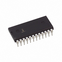
HI1-565ATD-2 Intersil, HI1-565ATD-2 Datasheet - Page 4

HI1-565ATD-2
Manufacturer Part Number
HI1-565ATD-2
Description
CONV D/A 12BIT 6.7MHZ 24-DIP
Manufacturer
Intersil
Datasheet
1.HI1-565AJD-5.pdf
(9 pages)
Specifications of HI1-565ATD-2
Number Of Bits
12
Data Interface
Parallel
Number Of Converters
1
Voltage Supply Source
Dual ±
Power Dissipation (max)
250mW
Operating Temperature
-55°C ~ 125°C
Mounting Type
Through Hole
Package / Case
24-DIP (0.600", 15.24mm)
Lead Free Status / RoHS Status
Lead free / RoHS Compliant
Settling Time
-
Available stocks
Company
Part Number
Manufacturer
Quantity
Price
Definitions of Specifications
Digital Inputs
The HI-565A accepts digital input codes in binary format and
may be user connected for any one of three binary codes.
Straight Binary, Two’s Complement (Note 5), or Offset
Binary, (See Operating Instructions).
NOTE:
Nonlinearity of a D/A converter is an important measure of
its accuracy. It describes the deviation from an ideal straight
line transfer curve drawn between zero (all bits OFF) and full
scale (all bits ON) (End Point Method).
Differential Nonlinearity for a D/A converter, it is the
difference between the actual output voltage change and the
ideal (1 LSB) voltage change for a one bit change in code. A
Differential Nonlinearity of ±1 LSB or less guarantees
monotonicity; i.e., the output always increases for an
increasing input.
Settling Time is the time required for the output to settle to
within the specified error band for any input code transition.
It is usually specified for a full scale or major carry transition,
settling to within ±0.5 LSB of final value.
Gain Drift is the change in full scale analog output over the
specified temperature range, expressed in parts per million
of full scale range per
measured with respect to 25
temperatures. Gain drift is calculated for both high (T
-25
by the respective change in temperature. The specification is
the larger of the two representing worst-case drift.
Offset Drift is the change in analog output with all bits OFF
over the specified temperature range expressed in parts per
million of full scale range per
is measured with respect to 25
temperatures. Offset Drift is calculated for both high (T
-25
by the respective change in temperature. The specification
given is the larger of the two, representing worst-case drift.
MSB...LSB
000...000
100...000
111...111
011...111
5. Invert MSB with external inverter to obtain Two’s Complement
DIGITAL
INPUT
o
o
Coding.
C) and low (25
C) and low ranges (25
1/2FS - 1 LSB
+FS - 1 LSB
STRAIGHT
BINARY
1
Zero
/
2
o
FS
C -T
o
C (ppm of FSR/
L
) ranges by dividing the offset error
TABLE 1.
o
ANALOG OUTPUT
C -T
o
o
C (ppm of FSR/
Zero - 1 LSB
+FS - 1 LSB
C at high (T
(Full Scale)
o
4
OFFSET
BINARY
C at high (T
L
Zero
-FS
) by dividing the gain error
o
C). Gain error is
H
H
) and low (T
) and low (T
COMPLEMENT
o
C). Offset error
Zero - 1 LSB
+FS - 1 LSB
(NOTE 5)
TWO'S
Zero
-FS
H
H
L
L
)
)
Power Supply Sensitivity is a measure of the change in
gain and offset of the D/A converter resulting from a change
in -15V or +15V supplies. It is specified under DC conditions
and expressed as parts per million of full scale range per
percent of change in power supply (ppm of FSR/%).
Compliance Voltage is the maximum output voltage range
that can be tolerated and still maintain its specified accuracy.
Compliance Limit implies functional operation only, and
makes no claims to accuracy.
Glitch a glitch on the output of a D/A converter is a transient
spike resulting from unequal internal ON-OFF switching
times. Worst case glitches usually occur at half-scale or the
major carry code transition from 011...1 to 100...0 or vice
versa. For example, if turn ON is greater than turn OFF for
011...1 to 100...0, an intermediate state of 000...0 exists,
such that, the output momentarily glitches toward zero
output. Matched switching times and fast switching will
reduce glitches considerably.
Detailed Description
Op Amp Selection
The Hl-565As current output may be converted to voltage
using the standard connections shown in Figures 1 and 2.
The choice of operational amplifier should be reviewed for
each application, since a significant trade-off may be made
between speed and accuracy.
For highest precision, use an HA-5135. This amplifier
contributes negligible error, but requires about 11µs to settle
within ±0.1% following a 10V step.
The Intersil HA-2600/05 is the best all-around choice for this
application, and it settles in 1.5µs (also to ±0.1% following a
10V step). Remember, settling time for the DAC amplifier
combination is the square root of t
are settling times for the DAC and amplifier.
No-Trim Operation
The Hl-565A will perform as specified without calibration
adjustments. To operate without calibration, substitute 50Ω
resistors for the 100Ω trimming potentiometers: In Figure 1
replace R2 with 50Ω also remove the network on pin 8 and
connect 50Ω to ground. For bipolar operation in Figure 2,
replace R3 and R4 with 50Ω resistors.
With these changes, performance is guaranteed as shown
under Specifications, “External Adjustments”. Typical unipolar
zero will be ±0.5 LSB plus the op amp offset.
The feedback capacitor, C, must be selected to minimize
settling time.
Calibration
Calibration provides the maximum accuracy from a
converter by adjusting its gain and offset errors to zero. For
the Hl-565A, these adjustments are similar whether the
current output is used, or whether an external op amp is
D
2
plus t
A
2
, where t
D
, t
A


