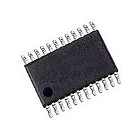
CAT5261YI-50-TE13 ON Semiconductor, CAT5261YI-50-TE13 Datasheet

CAT5261YI-50-TE13
Specifications of CAT5261YI-50-TE13
Related parts for CAT5261YI-50-TE13
CAT5261YI-50-TE13 Summary of contents
Page 1
Dual Digitally Programmable Potentiometers (DPP™) with 256 Taps and SPI Interface FEATURES Two linear-taper digitally programmable potentiometers 256 resistor taps per potentiometer End to end resistance 50 kΩ or 100 kΩ Potentiometer control and memory access via SPI interface Low ...
Page 2
CAT5261 PIN DESCRIPTIONS SI: Serial Input SI is the serial data input pin. This pin is used to input all opcodes, byte addresses and data to be written to the CAT5261. Input data is latched on the rising edge of ...
Page 3
SERIAL BUS PROTOCOL The CAT5261 supports the SPI bus data transmission protocol. The synchronous Serial Peripheral Interface (SPI) helps the CAT5261 to interface directly with many of today's popular microcontrollers. DEVICE OPERATION The CAT5261 is two resistor arrays integrated with ...
Page 4
CAT5261 ABSOLUTE MAXIMUM RATINGS Parameters Temperature Under Bias Storage Temperature Voltage on Any Pin with Respect to Ground V with Respect to Ground CC Package Power Dissipation Capability (T Lead Soldering Temperature (10 s) Wiper Current RECOMMENDED OPERATING CONDITIONS Parameters ...
Page 5
D.C. OPERATING CHARACTERISTICS +6.0 V, unless otherwise specified. CC Symbol Parameter I Power Supply Current CC1 Power Supply Current I CC2 Non-volatile WRITE I Standby Current ( Input Leakage Current LI I ...
Page 6
CAT5261 (1)(2) POWER UP TIMING Symbol Parameter t Power-up to Read Operation PUR t Power-up to Write Operation PUW WIPER TIMING Symbol Parameter t Wiper Response Time After Power Supply Stable WRPO t Wiper Response Time After Instruction Issued WRL ...
Page 7
Timing Figure 2. HOLD CS SCK HOLD SO INSTRUCTION AND REGISTER DESCRIPTION DEVICE TYPE / ADDRESS BYTE The first byte sent to the CAT5261 from the master/ processor is called the Device Address Byte. The most significant four bits ...
Page 8
CAT5261 WIPER CONTROL AND DATA REGISTERS Wiper Control Register (WCR) The CAT5261 contains two 8-bit Wiper Control Registers, one for each potentiometer. The Wiper Control Register output is decoded to select one of 256 switches along its resistor array. The ...
Page 9
The basic sequence of the three byte instructions is illustrated in Figure 8. These three-byte instructions exchange data between the WCR and one of the Data Registers. The WCR controls the position of the wiper. The response of the wiper ...
Page 10
CAT5261 Figure 10. Increment/Decrement INC/DEC Command Issued SCK INSTRUCTION FORMAT Read Wiper Control Register (WCR) DEVICE ADDRESSES ¯¯¯ Write Wiper Control Register (WCR) DEVICE ADDRESSES ¯¯¯ ...
Page 11
Global Transfer Data Register (DR) to Wiper Control Register (WCR) DEVICE ADDRESSES ¯¯¯ Global Transfer Wiper Control Register (WCR) to Data Register (DR) DEVICE ADDRESSES ¯¯¯ ...
Page 12
CAT5261 PACKAGE OUTLINE DRAWINGS SOIC 24-Lead 300 mils ( PIN#1 IDENTIFICATION TOP VIEW D A SIDE VIEW Notes: (1) All dimensions in millimeters. Angles in degrees. (2) Complies with JEDEC specification MS-013. Doc. No. MD-2122 Rev. G SYMBOL ...
Page 13
TSSOP 24-Lead 4.4 mm (Y) e TOP VIEW SIDE VIEW Notes: (1) All dimensions in millimeters. Angles in degrees. (2) Complies with JEDEC specification MO-153. © 2009 SCILLC. All rights reserved. Characteristics subject to change without notice ...
Page 14
... Orderable Part Number Resistance (kΩ) CAT5261WI-50-T1 CAT5261WI-00-T1 CAT5261YI-50-T2 CAT5261YI-00-T2 CAT5261WI50 CAT5261WI00 CAT5261YI50 CAT5261YI00 Notes: (1) All packages are RoHS-compliant (Lead-free, Halogen-free). (2) The device used in the above example is a CAT526159WI-00-T1 (SOIC, Industrial Temperature, 100 Doc. No. MD-2122 Rev. G (1) I Temperature Range I = Industrial (-40ºC to 85ºC) ...
Page 15
... E Update Instruction Format – Read Data Register (DR) and Write Data Register (DR) 24-Nov-08 F Change logo and fine print to ON Semiconductor 05-Aug-09 G Update Ordering Information table ON Semiconductor and are registered trademarks of Semiconductor Components Industries, LLC (SCILLC). SCILLC reserves the right to make changes without further notice to any products herein ...


