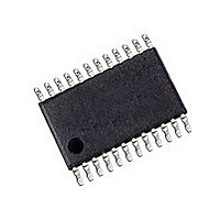
CAT5261YI-50-TE13 ON Semiconductor, CAT5261YI-50-TE13 Datasheet - Page 4

CAT5261YI-50-TE13
Manufacturer Part Number
CAT5261YI-50-TE13
Description
Manufacturer
ON Semiconductor
Datasheet
1.CAT5261YI-50-TE13.pdf
(15 pages)
Specifications of CAT5261YI-50-TE13
Number Of Elements
2
# Of Taps
256
Resistance (max)
50KOhm
Power Supply Requirement
Single
Interface Type
Serial (SPI)
Single Supply Voltage (typ)
3.3/5V
Dual Supply Voltage (typ)
Not RequiredV
Single Supply Voltage (min)
2.5V
Single Supply Voltage (max)
6V
Dual Supply Voltage (min)
Not RequiredV
Dual Supply Voltage (max)
Not RequiredV
Operating Temp Range
-40C to 85C
Operating Temperature Classification
Industrial
Mounting
Surface Mount
Pin Count
24
Lead Free Status / Rohs Status
Compliant
CAT5261
ABSOLUTE MAXIMUM RATINGS
RECOMMENDED OPERATING CONDITIONS
POTENTIOMETER CHARACTERISTICS
(Over recommended operating conditions unless otherwise stated.)
Notes:
(1) Stresses above those listed under “Absolute Maximum Ratings” may cause permanent damage to the device. These are stress ratings
(2) The minimum DC input voltage is –0.5 V. During transitions, inputs may undershoot to –2.0 V for periods of less than 20 ns. Maximum DC
(3) Latch-up protection is provided for stresses up to 100 mA on address and data pins from –1 V to V
(4) This parameter is tested initially and after a design or process change that affects the parameter.
(5) Absolute linearity is utilized to determine actual wiper voltage versus expected voltage as determined by wiper position when used as a potentiometer.
(6) Relative linearity is utilized to determine the actual change in voltage between two successive tap positions when used as a potentio-
(7) LSB = R
(8) n = 0, 1, 2, ..., 255
Doc. No. MD-2122 Rev. G
Parameters
Temperature Under Bias
Storage Temperature
Voltage on Any Pin with Respect to Ground
V
Package Power Dissipation Capability (T
Lead Soldering Temperature (10 s)
Wiper Current
Parameters
V
Industrial Temperature
C
Symbol
TC
TC
CC
CC
H
V
only, and functional operation of the device at these or any other conditions outside of those listed in the operational sections of this
specification is not implied. Exposure to any absolute maximum rating for extended periods may affect device performance and reliability.
voltage on output pins is V
meter. It is a measure of the error in step size.
R
R
/C
VN
R
R
TERM
I
fc
POT
POT
RATIO
with Respect to Ground
RPOT
W
W
W
L
/C
W
TOT
/ 255 or (R
Parameter
Potentiometer Resistance (-00)
Potentiometer Resistance (-50)
Potentiometer Resistance
Tolerance
R
Power Rating
Wiper Current
Wiper Resistance
Wiper Resistance
Voltage on any R
Noise
Resolution
Absolute Linearity
Relative Linearity
Temperature Coefficient of R
Ratiometric Temp. Coefficient
Potentiometer Capacitances
Frequency Response
POT
Matching
H
- R
CC
L
) / 255, single pot
+0.5 V, which may overshoot to V
H
(6)
(5)
or R
(1)
L
Pin
POT
A
= 25ºC)
(1) (2)
25°C, each pot
I
I
(4)
Rw(n)(actual)-R(n)(expected)
Rw(n+1)-[Rw(n)+LSB]
(4)
(4)
(4)
R
Test Conditions
W
W
POT
= ±3 mA @ V
= ±3 mA @ V
= 50 kΩ
CC
+2.0 V for periods of less than 20 ns.
4
(4)
CC
CC
= 3 V
= 5 V
(8)
(8)
Min
0
-2.0 to +V
CC
+1 V.
+2.5 to +6.0
-55 to +125
-65 to +150
-0.2 to +7.0
Characteristics subject to change without notice
-40 to +85
10/10/25
Ratings
Ratings
Limits
±300
Typ.
100
200
100
300
0.4
0.4
1.0
50
±6
CC
© 2009 SCILLC. All rights reserved.
+ 2.0
Max
±0.2
±20
300
150
V
50
±3
±1
20
1
CC
ppm/ºC
ppm/ºC
nV
LSB
LSB
Units
Units
Units
MHz
mW
mA
mA
kΩ
kΩ
ºC
°C
ºC
°C
pF
W
%
%
%
V
V
Ω
Ω
V
V
√
Hz
(7)
(7)


