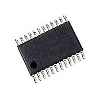
CAT5261YI-50-TE13 ON Semiconductor, CAT5261YI-50-TE13 Datasheet - Page 2

CAT5261YI-50-TE13
Manufacturer Part Number
CAT5261YI-50-TE13
Description
Manufacturer
ON Semiconductor
Datasheet
1.CAT5261YI-50-TE13.pdf
(15 pages)
Specifications of CAT5261YI-50-TE13
Number Of Elements
2
# Of Taps
256
Resistance (max)
50KOhm
Power Supply Requirement
Single
Interface Type
Serial (SPI)
Single Supply Voltage (typ)
3.3/5V
Dual Supply Voltage (typ)
Not RequiredV
Single Supply Voltage (min)
2.5V
Single Supply Voltage (max)
6V
Dual Supply Voltage (min)
Not RequiredV
Dual Supply Voltage (max)
Not RequiredV
Operating Temp Range
-40C to 85C
Operating Temperature Classification
Industrial
Mounting
Surface Mount
Pin Count
24
Lead Free Status / Rohs Status
Compliant
CAT5261
PIN DESCRIPTIONS
SI: Serial Input
SI is the serial data input pin. This pin is used
to input all opcodes, byte addresses and data
to be written to the CAT5261. Input data is
latched on the rising edge of the serial clock.
SO: Serial Output
SO is the serial data output pin. This pin is
used to transfer data out of the CAT5261.
During a read cycle, data is shifted out on the
falling edge of the serial clock.
SCK: Serial Clock
SCK is the serial clock pin. This pin is used to
synchronize the communication between the
microcontroller and the CAT5261. Opcodes,
byte addresses or data present on the SI pin
are latched on the rising edge of the SCK.
Data on the SO pin is updated on the falling
edge of the SCK.
A0, A1: Device Address Inputs
These inputs set the device address when
addressing multiple devices. A total of four
devices can be addressed on a single bus. A
match in the slave address must be made
with the address input in order to initiate
communication with the CAT5261.
R
The R
terminal
potentiometer.
R
The RW pins are equivalent to the wiper
terminal of a mechanical potentiometer.
¯¯¯ : Chip Select
¯¯¯ is the Chip select pin. CS
the CAT5261 and CS
CAT5261. CS
(unless an internal write operation is underway). The CAT5261 draws ZERO current in the Standby mode. A high
to low transition on CS
valid write sequence is what initiates an internal write cycle.
¯¯¯ : Write Protect
WP
¯¯¯ is the Write Protect pin. The Write Protect pin will allow normal read/write operations when held high. When
WP
¯¯¯ is tied low, all non-volatile write operations to the Data registers are inhibited (change of wiper control register
WP
is allowed). WP
already been initiated, WP
HOLD
The HOLD
having to retransmit entire sequence at a later time. To pause, HOLD
SO pin is in a high impedance state during the time the part is paused, and transitions on the SI pins will be
ignored. To resume communication, HOLD
time this function is not being used.) HOLD
¯¯¯ : Write Protect Input
WP
The WP
and when tied high or left floating normal read/write operations are allowed. See Write Protection on page 6 for
more details.
Doc. No. MD-2122 Rev. G
¯¯¯¯¯ : Hold
CS
CS
H
W
, R
: Wiper
¯¯¯ pin when tied low prevents non-volatile writes to the device (change of wiper control register is allowed)
¯¯¯¯¯ pin is used to pause transmission to the CAT5261 while in the middle of a serial sequence without
L
: Resistor End Points
H
and R
connections
¯¯¯ high takes the SO output pin to high impedance and forces the devices into a Standby mode
¯¯¯ going low while CS
L
pins are equivalent to the
¯¯¯ is required prior to any sequence being initiated. A low to high transition on CS
¯¯¯ high disables the
¯¯¯ going low will have no effect on any write operation.
on
¯¯¯ low enables
a
¯¯¯ is still low will interrupt a write to the registers. If the internal write cycle has
mechanical
¯¯¯¯¯ may be tied high directly to V
¯¯¯¯¯ is brought high, while SCK is low. (HOLD
Pin #
10
11
12
13
14
15
16
17
18
19
20
21
22
23
24
1
2
3
4
5
6
7
8
9
2
Name
¯¯¯¯¯
HOLD
GND
SCK
R
R
V
¯¯¯
¯¯¯
WP
SO
NC
NC
NC
NC
R
R
R
NC
NC
NC
NC
R
CS
A0
A1
SI
CC
W0
W1
L0
H0
L1
H1
¯¯¯¯¯ must be brought low while SCK is low. The
Function
Serial Data Output
Device Address, LSB
No Connect
No Connect
No Connect
No Connect
Supply Voltage
Low Reference Terminal for Potentiometer 0
High Reference Terminal for Potentiometer 0
Wiper Terminal for Potentiometer 0
Chip Select
Write Protection
Serial Input
Device Address
Low Reference Terminal for Potentiometer 1
High Reference Terminal for Potentiometer 1
Wiper Terminal for Potentiometer 1
Ground
No Connect
No Connect
No Connect
No Connect
Bus Serial Clock
Hold
CC
or tied to V
¯¯¯¯¯ should be held high any
Characteristics subject to change without notice
CC
through a resistor.
© 2009 SCILLC. All rights reserved.
¯¯¯ after a


