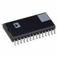
AD1859JR Analog Devices Inc, AD1859JR Datasheet - Page 6

AD1859JR
Manufacturer Part Number
AD1859JR
Description
IC DAC STEREO SNGL-SUP 5V 28SOIC
Manufacturer
Analog Devices Inc
Datasheet
1.AD1859JR.pdf
(16 pages)
Specifications of AD1859JR
Rohs Status
RoHS non-compliant
Number Of Bits
18
Data Interface
DSP, I²S, Serial, SPI™
Number Of Converters
2
Voltage Supply Source
Analog and Digital
Power Dissipation (max)
330mW
Operating Temperature
-40°C ~ 105°C
Mounting Type
Surface Mount
Package / Case
28-SOIC (7.5mm Width)
Settling Time
-
Available stocks
Company
Part Number
Manufacturer
Quantity
Price
Company:
Part Number:
AD1859JR
Manufacturer:
AD
Quantity:
4 530
Company:
Part Number:
AD1859JRS
Manufacturer:
AD
Quantity:
5 510
Part Number:
AD1859JRS
Manufacturer:
ADI/亚德诺
Quantity:
20 000
Part Number:
AD1859JRSZ
Manufacturer:
ADI/亚德诺
Quantity:
20 000
Part Number:
AD1859JRZ
Manufacturer:
ADI/亚德诺
Quantity:
20 000
AD1859
Analog Signals
Pin Name
FILT
FGND
CMOUT
OUTL
OUTR
EMPL
EMPR
Number
28
27
1
4
25
3
26
I/O Description
O
I
O
O
O
O
O
Voltage reference filter capacitor
connection. Bypass and decouple
the voltage reference with paral-
lel 10 F and 0.1 F capacitors
to the FGND pin.
Voltage reference filter ground.
Use exclusively for bypassing and
decoupling of the FILT pin
(voltage reference).
Voltage reference common-mode
output. Should be decoupled
with 10 F capacitor to the AGND
pin or plane. This output is available
externally for dc-coupling and level-
shifting. CMOUT should not have
any signal dependent load, or where
it will sink or source current.
Left channel line level analog output.
Right channel line level analog output.
De-emphasis switch connection
for the left channel. Can be left
unconnected if de-emphasis is not
required in the target application.
De-emphasis switch connection
for the right channel. Can be left
unconnected if de-emphasis is not
required in the target application.
PIN DESCRIPTIONS
–6–
Control and Clock Signals
Pin Name
PD/RST
DEEMP
MUTE
XTALI/
MCLK
XTALO
Power Supply Connections and Miscellaneous
Pin Name
AV
AGND
DV
DGND
NC
DD
DD
Number
11
2
7
16
15
Number
23
6
17
18
5, 22, 24
I
I
I
O
I/O Description
I
I/O Description
I
I
I
I
Power down/reset. The AD1859 is
placed in a low power consumption
“sleep” mode when this pin is held
LO. The AD1859 is reset on the
rising edge of this signal. The serial
control port registers are reset to
their default values. Connect HI
for normal operation.
De-emphasis. An external analog de-
emphasis circuit network is enabled
when this input signal is HI. This
circuit is typically used to impose a
50/15 s (or perhaps the CCITT
J.17) response characteristic on the
output audio spectrum.
Mute. Assert HI to mute both
stereo analog outputs of the AD1859.
Deassert LO for normal operation.
Crystal input or master clock input.
Connect to one side of a quartz
crystal to this input, or connect to
an external clock source to over-
drive the on-chip oscillator.
Crystal output. Connect to other
side of a quartz crystal. Do not con-
nect if using the XTALI/MCLK
pin with an external clock source.
Analog Ground.
Digital Ground.
Analog Power Supply. Connect
to analog +5 V supply.
Digital Power Supply. Connect
to digital +5 V supply.
No Connect. Reserved. Do not
connect.
REV. A


