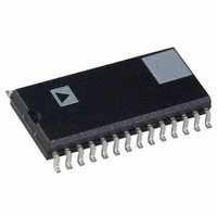
AD1859JR Analog Devices Inc, AD1859JR Datasheet - Page 9

AD1859JR
Manufacturer Part Number
AD1859JR
Description
IC DAC STEREO SNGL-SUP 5V 28SOIC
Manufacturer
Analog Devices Inc
Datasheet
1.AD1859JR.pdf
(16 pages)
Specifications of AD1859JR
Rohs Status
RoHS non-compliant
Number Of Bits
18
Data Interface
DSP, I²S, Serial, SPI™
Number Of Converters
2
Voltage Supply Source
Analog and Digital
Power Dissipation (max)
330mW
Operating Temperature
-40°C ~ 105°C
Mounting Type
Surface Mount
Package / Case
28-SOIC (7.5mm Width)
Settling Time
-
Available stocks
Company
Part Number
Manufacturer
Quantity
Price
Company:
Part Number:
AD1859JR
Manufacturer:
AD
Quantity:
4 530
Company:
Part Number:
AD1859JRS
Manufacturer:
AD
Quantity:
5 510
Part Number:
AD1859JRS
Manufacturer:
ADI/亚德诺
Quantity:
20 000
Part Number:
AD1859JRSZ
Manufacturer:
ADI/亚德诺
Quantity:
20 000
Part Number:
AD1859JRZ
Manufacturer:
ADI/亚德诺
Quantity:
20 000
REV. A
Figure 3 shows the I
channel, and HI for the right channel. Data is valid on the rising
edge of BCLK. The MSB is left-justified to an LRCLK transition
but with a single BCLK period delay. The I
can be used in either the 16-bit or the 18-bit input mode.
Figure 4 shows the left-justified mode. LRCLK is HI for the
left channel, and LO for the right channel. Data is valid on the
rising edge of BCLK. The MSB is left-justified to an LRCLK
transition, with no MSB delay. The left-justified mode can be
used in either the 16-bit or the 18-bit input mode.
Figure 5 shows the left-justified DSP serial port style mode.
LRCLK must pulse HI for at least one bit clock period before
the MSB of the left channel is valid, and LRCLK must pulse HI
again for at least one bit clock period before the MSB of the
right channel is valid. Data is valid on the falling edge of
BCLK. The left-justified DSP serial port style mode can be
used in either the 16-bit or the 18-bit input mode. Note that in
this mode, it is the responsibility of the DSP to ensure that the
left data is transmitted with the first LRCLK pulse, and that the
right data is transmitted with the second LRCLK pulse, and
that synchronism is maintained from that point forward.
SDATA
LRCLK
SDATA
LRCLK
SDATA
LRCLK
INPUT
INPUT
INPUT
INPUT
INPUT
INPUT
INPUT
INPUT
INPUT
BCLK
BCLK
BCLK
MSB
2
S-justified mode. LRCLK is LO for the left
MSB-1
MSB
MSB
SDATA
LRCLK
INPUT
INPUT
INPUT
BCLK
MSB-2
MSB-1
MSB-1
MSB-2
LSB
MSB
LEFT CHANNEL
LSB+2
LSB+2
Figure 5. Left-Justified DSP Serial Port Style Mode
LEFT CHANNEL
MSB-1 MSB-2
LEFT CHANNEL
LSB+1
LEFT CHANNEL
LSB+2
LSB+1
2
S-justified mode
LSB+1
LSB
LSB
Figure 6. 32
Figure 4. Left-Justified Mode
Figure 3. I
LSB
LSB+2
LSB+1
2
S-Justified Mode
–9–
LSB
F
S
Packed Mode
Note that in 16-bit input mode, the AD1859 is capable of a 32
justified to an LRCLK transition, and the LSB is right-justified
to an LRCLK transition. LRCLK is HI for the left channel,
and LO for the right channel. Data is valid on the rising edge of
BCLK. Packed mode can be used when the AD1859 is pro-
grammed in either right-justified or left-justified mode. Packed
mode is shown in Figure 6.
Serial Control Port
The AD1859 serial control port is SPI compatible. SPI
(Serial Peripheral Interface) is a serial port protocol popularized
by Motorola’s family of microcomputer and microcontroller
products. The write-only serial control port gives the user ac-
cess to channel specific mute and attenuation. The AD1859
serial control port consists of three signals, control clock CCLK
(Pin 19), control data CDATA (Pin 20), and control latch
CLATCH (Pin 21). The control data input (CDATA) must be
valid on the control clock (CCLK) rising edge, and the control
clock (CCLK) must only make a LO to HI transition when
there is valid data. The control latch (CLATCH) must make a
LO to HI transition after the LSB has been clocked into the
AD1859, while the control clock (CCLK) is inactive. The tim-
ing relation between these signals is shown in Figure 7.
MSB
MSB
F
RIGHT CHANNEL
S
MSB-1
MSB
MSB
MSB-1 MSB-2
BCLK frequency “packed mode” where the MSB is left-
MSB-2
MSB-1
MSB-1
MSB-2
RIGHT CHANNEL
LSB+2
LSB+2
LSB+2
RIGHT CHANNEL
LSB+2
LSB+1
LSB+1
LSB+1
RIGHT CHANNEL
LSB+1
LSB
LSB
LSB
LSB
MSB
MSB-1
AD1859
MSB
MSB
MSB-1
MSB-1
MSB


