0W888-002-XTP ON Semiconductor, 0W888-002-XTP Datasheet - Page 11
0W888-002-XTP
Manufacturer Part Number
0W888-002-XTP
Description
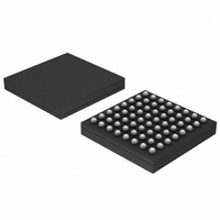
DSP BELASIGNA 250 AUDIO 64LFBGA
Manufacturer
ON Semiconductor
Series
BelaSigna® 250r
Type
Floating Pointr
Datasheet
1.B250W48A106XXG.pdf
(33 pages)
Specifications of 0W888-002-XTP
Interface
I²C, I²S, PCM, SPI, UART
Clock Rate
50MHz
On-chip Ram
42kB
Voltage - I/o
1.0V, 2.0V
Voltage - Core
1.00V, 2.00V
Operating Temperature
-40°C ~ 85°C
Mounting Type
Surface Mount
Package / Case
64-LFBGA
Package
64LFBGA
Numeric And Arithmetic Format
Fixed-Point
Ram Size
16 KB
Lead Free Status / RoHS Status
Lead free / RoHS Compliant
Non-volatile Memory
-
Available stocks
Company
Part Number
Manufacturer
Quantity
Price
Company:

Part Number:
0W888-002-XTP
Manufacturer:
ON Semiconductor
Quantity:
10 000


Solder Ball Composition
package is SAC105.
Recommended Design Guidelines
coupled with its superior audio performance and low cost
makes it a preferred package for portable audio devices.
processing in a single system. Due to the mixed−signal
nature of this system, the careful design of the printed circuit
board (PCB) layout is critical to maintain the high audio
fidelity of BelaSigna 250. To avoid coupling noise into the
audio signal path, keep the digital traces away from the
analog traces. To avoid electrical feedback coupling, isolate
the input traces from the output traces.
CSP package is constrained in ways that will factor into
design decisions. The CSP will only operate in HV mode,
and therefore requires a 1.8 V operating voltage. The
number of pins is reduced to 48 (compared to 51 active pins
on the LFBGA). This reduction eliminates access to GNDO
(connected to GNDC) and AI_RC (connected to AGND).
ON Semiconductor recommends Solder−on−Pad (SoP)
surface finish. With SoP, the solder mask opening should be
solder mask−defined and copper pad geometry will be
dictated by the PCB vendor’s design requirements.
of screened solder paste (#5) should be less than
0.0008 mm
then following conditions must be met:
Table 5. WLCSP PIN DESCRIPTIONS
The solder ball composition of the BelaSigna 250 WLCSP
The small size of the BelaSigna 250 WLCSP package
BelaSigna 250 is designed to allow both digital and analog
In order to achieve the highest level of miniaturization, the
For PCB manufacture with BelaSigna 250 WLCSP,
Alternative surface finishes are ENiG and OSP; volume
C6
C7
C8
D6
A8
B7
B8
F8
3
. If no pre−screening of solder paste is used,
GPIO[9]/LSAD[5]/UART_RX
GPIO[10]/UCLK
GPIO[11]/PCM_CLK
GPIO[12]/PCM_SERI
GPIO[13]/PCM_SERO
GPIO[14]/PCM_FRAME
GPIO[15]
RESERVED
(continued)
http://onsemi.com
General purpose input or output/ low−speed A/D input/
UART output
General purpose input or output/ user clock
General purpose input or output/ PCM clock
General purpose input or output/ PCM serial input
General purpose input or output/ PCM serial output
General purpose input or output/ PCM frame
General purpose input or output
Leave disconnected
11
land pattern CAD files to assist your PCB design upon
request.
Recommended Ground Design Strategy
analog ground plane (AGND) and the digital ground plane
(DGND). These two planes should be connected together at
a single point, known as the star point. The star point should
be located at the ground terminal of a capacitor on the output
of the power regulator as illustrated in Figure 1.
circuits and should be placed under digital circuits. The
AGND plane should be kept as noise−free as possible. It is
used as the ground return for analog circuits and it should
surround analog components and pins. It should not be
connected to or placed under any noisy circuits such as RF
chips, switching supplies or digital pads of BelaSigna 250
itself. Analog ground returns associated with the audio
output stage should connect back to the star point on separate
individual traces.
strategy, see Table 6 and Table 7.
ground planes impractical. In this case a star configuration
strategy should be used. Each analog ground return should
connect to the star point with separate traces.
ON Semiconductor can provide BelaSigna 250 WLCSP
The ground plane should be partitioned into two: the
The DGND plane is used as the ground return for digital
For more information on the recommended ground design
In some designs, space constraints may make separate
1. the solder mask opening should be >0.3 mm in
2. the copper pad will have 0.25 mm diameter, and
3. soldermask thickness should be less than 1 mil
diameter,
thick above the copper surface.
N/A
I/O
I/O
I/O
I/O
I/O
I/O
I/O
A/D
N/A
D
D
D
D
D
D
Related parts for 0W888-002-XTP
Image
Part Number
Description
Manufacturer
Datasheet
Request
R

Part Number:
Description:
ON Semiconductor [VOLTAGE REGULATOR]
Manufacturer:
ON Semiconductor
Datasheet:
Part Number:
Description:
357-036-542-201 CARDEDGE 36POS DL .156 BLK LOPRO
Manufacturer:
ON Semiconductor
Datasheet:
Part Number:
Description:
357-036-542-201 CARDEDGE 36POS DL .156 BLK LOPRO
Manufacturer:
ON Semiconductor
Datasheet:
Part Number:
Description:
357-036-542-201 CARDEDGE 36POS DL .156 BLK LOPRO
Manufacturer:
ON Semiconductor
Datasheet:
Part Number:
Description:
357-036-542-201 CARDEDGE 36POS DL .156 BLK LOPRO
Manufacturer:
ON Semiconductor
Datasheet:
Part Number:
Description:
357-036-542-201 CARDEDGE 36POS DL .156 BLK LOPRO
Manufacturer:
ON Semiconductor
Datasheet:
Part Number:
Description:
357-036-542-201 CARDEDGE 36POS DL .156 BLK LOPRO
Manufacturer:
ON Semiconductor
Datasheet:
Part Number:
Description:
357-036-542-201 CARDEDGE 36POS DL .156 BLK LOPRO
Manufacturer:
ON Semiconductor
Datasheet:
Part Number:
Description:
357-036-542-201 CARDEDGE 36POS DL .156 BLK LOPRO
Manufacturer:
ON Semiconductor
Datasheet:
Part Number:
Description:
357-036-542-201 CARDEDGE 36POS DL .156 BLK LOPRO
Manufacturer:
ON Semiconductor
Datasheet:
Part Number:
Description:
357-036-542-201 CARDEDGE 36POS DL .156 BLK LOPRO
Manufacturer:
ON Semiconductor
Datasheet:
Part Number:
Description:
Manufacturer:
ON Semiconductor
Datasheet:
Part Number:
Description:
Manufacturer:
ON Semiconductor
Datasheet:
Part Number:
Description:
Manufacturer:
ON Semiconductor
Datasheet: