0W888-002-XTP ON Semiconductor, 0W888-002-XTP Datasheet - Page 23
0W888-002-XTP
Manufacturer Part Number
0W888-002-XTP
Description
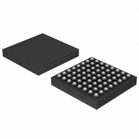
DSP BELASIGNA 250 AUDIO 64LFBGA
Manufacturer
ON Semiconductor
Series
BelaSigna® 250r
Type
Floating Pointr
Datasheet
1.B250W48A106XXG.pdf
(33 pages)
Specifications of 0W888-002-XTP
Interface
I²C, I²S, PCM, SPI, UART
Clock Rate
50MHz
On-chip Ram
42kB
Voltage - I/o
1.0V, 2.0V
Voltage - Core
1.00V, 2.00V
Operating Temperature
-40°C ~ 85°C
Mounting Type
Surface Mount
Package / Case
64-LFBGA
Package
64LFBGA
Numeric And Arithmetic Format
Fixed-Point
Ram Size
16 KB
Lead Free Status / RoHS Status
Lead free / RoHS Compliant
Non-volatile Memory
-
Available stocks
Company
Part Number
Manufacturer
Quantity
Price
Company:

Part Number:
0W888-002-XTP
Manufacturer:
ON Semiconductor
Quantity:
10 000


Clock−Generation Circuitry
flexibility in the control of peripherals, the selection of
sampling frequencies and the configuration of interface
communication speeds. The five clock domains are as
follows in Table 11. The base clock for all operations on the
to a frequency of 5.12 MHz. To operate properly using this
internal clock, BelaSigna 250 has to be calibrated, and the
calibration values are to be stored within a non−volatile
memory (usually an SPI EEPROM). When calibration isn’t
possible, BelaSigna 250 can operate with an externally
supplied SYS_CLK, in this case, it is qualified for operation
up to 50 MHz.
depends on MCLK. When MCLK is 1.28 MHz, sampling
frequencies up to 20 kHz can be selected. When MCLK is
1.92 MHz sampling frequencies up to 30 kHz can be
selected. For MCLK equal to 2.56 MHz sampling
frequencies up to 40 kHz can be selected. For MCLK equal
to 3.84 MHz, sampling frequencies up to 60 kHz can be
selected.
operations to be performed at a frequency slower than
SYS_CLK. This feature allows the dynamic current
consumption related to the digital blocks to be “spread” over
a longer period of time, smoothing the system’s dynamic
current draw, which can affect the audio signal.
signal to an external component, independently from the
EXT_CLK pin functionality. It can be derived from
SYS_CLK with a variety of derivation factors, or can be
connected to MCLK or even PCLK. One instance in which
it is beneficial to use this feature is when a continuous
external clock output is required but when EXT_CLK is
already being used to provide SYS_CLK to BelaSigna 250.
Power Supply Unit
Voltage Modes
modes: high, low and double voltage. These modes allow
BelaSigna 250 to integrate into a wider variety of devices
with a range of voltage supplies and communications levels.
The power supply modes are described below:
•
Table 11. CLOCK DOMAINS
SYS_CLK
MCLK
PCLK
WOLACLK
UCLK
The chip operates with five clock domains to provide
The internal RC oscillator is characterized to operate up
The sampling frequency for all A/D and D/A converters
The WOLA clock (WCLK) feature allows WOLA
The user clock (UCLK) can be used to provide a clock
BelaSigna 250 can operate in three different power supply
High voltage (HV) power supply mode: BelaSigna
250 operates from a nominal supply of 1.8 V on VBAT,
Clock Name
System clock
Main clock
Peripheral clock
WOLA clock
User clock
Description
All on−chip processors such as RCore, WOLA, IOP
All A/D and D/A converters
Debug port, remote control, watchdog timer
WOLA module computations
Can be programmed to provide a dedicated clock for an external device
http://onsemi.com
23
BelaSigna 250 chip is the system clock (SYS_CLK). This
clock may be acquired from one of three sources: the main
on−chip oscillator, the system standby clock or an external
clock signal.
•
•
Power−on−Reset (POR) and Booting Sequence
into known default states. During the power−on procedure,
all audio outputs are muted; all RCore registers and all
control registers (analog and digital) are set to default
values. (Please contact ON Semiconductor for more
information on default values associated with each control
register.)
program ROM begins loading the bootloader from an
external EEPROM 200 ms after power is applied to the chip.
At POR, all control registers and RCore registers are put
BelaSigna 250 boots in a two−stage boot sequence. The
but this can scale depending on available supply. All
digital sections of the system, including digital I/O
pads, run from the same voltage as supplied on VBAT.
This mode is preferable in designs where a very stable
supply is available and BelaSigna 250 will be interfacing
to other digital systems at the same voltage. This mode
is also necessary for higher than 5.12 MHz system
clocks.
Low voltage (LV) power supply mode: BelaSigna 250
operates from a nominal supply of 1.25 V. The WOLA,
the RCore and all digital I/O pads run from a 1 V
regulated supply. The low voltage operation of the
processing cores is very power−efficient, but the system
clock should be kept under 5.12 MHz to ensure proper
operation.
Double voltage (DV) power supply mode: BelaSigna
250 operates from a nominal supply of 1.25 V. The
WOLA, the RCore and all digital I/O pads run from the
on−chip charge pump which regulates internal voltage
up to 2 V. This allows BelaSigna 250 to communicate
with higher voltage systems like a 1.8 V EEPROM
when running on a lower supply voltage. However, a
specific level translation mechanism has been designed
to allow BelaSigna 250 to communicate with an SPI
EEPROM in low voltage mode as well. This voltage
mode is not suitable for normal operation, processing in
this mode may result in audible audio artifacts. Most
BelaSigna 250 applications run in high voltage mode.
Used For
Related parts for 0W888-002-XTP
Image
Part Number
Description
Manufacturer
Datasheet
Request
R

Part Number:
Description:
ON Semiconductor [VOLTAGE REGULATOR]
Manufacturer:
ON Semiconductor
Datasheet:
Part Number:
Description:
357-036-542-201 CARDEDGE 36POS DL .156 BLK LOPRO
Manufacturer:
ON Semiconductor
Datasheet:
Part Number:
Description:
357-036-542-201 CARDEDGE 36POS DL .156 BLK LOPRO
Manufacturer:
ON Semiconductor
Datasheet:
Part Number:
Description:
357-036-542-201 CARDEDGE 36POS DL .156 BLK LOPRO
Manufacturer:
ON Semiconductor
Datasheet:
Part Number:
Description:
357-036-542-201 CARDEDGE 36POS DL .156 BLK LOPRO
Manufacturer:
ON Semiconductor
Datasheet:
Part Number:
Description:
357-036-542-201 CARDEDGE 36POS DL .156 BLK LOPRO
Manufacturer:
ON Semiconductor
Datasheet:
Part Number:
Description:
357-036-542-201 CARDEDGE 36POS DL .156 BLK LOPRO
Manufacturer:
ON Semiconductor
Datasheet:
Part Number:
Description:
357-036-542-201 CARDEDGE 36POS DL .156 BLK LOPRO
Manufacturer:
ON Semiconductor
Datasheet:
Part Number:
Description:
357-036-542-201 CARDEDGE 36POS DL .156 BLK LOPRO
Manufacturer:
ON Semiconductor
Datasheet:
Part Number:
Description:
357-036-542-201 CARDEDGE 36POS DL .156 BLK LOPRO
Manufacturer:
ON Semiconductor
Datasheet:
Part Number:
Description:
357-036-542-201 CARDEDGE 36POS DL .156 BLK LOPRO
Manufacturer:
ON Semiconductor
Datasheet:
Part Number:
Description:
Manufacturer:
ON Semiconductor
Datasheet:
Part Number:
Description:
Manufacturer:
ON Semiconductor
Datasheet:
Part Number:
Description:
Manufacturer:
ON Semiconductor
Datasheet: