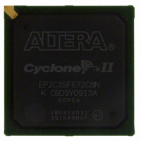
EP2C35F672C8N Altera, EP2C35F672C8N Datasheet - Page 70

EP2C35F672C8N
Manufacturer Part Number
EP2C35F672C8N
Description
IC CYCLONE II FPGA 33K 672-FBGA
Manufacturer
Altera
Series
Cyclone® IIr
Datasheet
1.EP2C5T144C8N.pdf
(168 pages)
Specifications of EP2C35F672C8N
Number Of Logic Elements/cells
33216
Number Of Labs/clbs
2076
Total Ram Bits
483840
Number Of I /o
475
Voltage - Supply
1.15 V ~ 1.25 V
Mounting Type
Surface Mount
Operating Temperature
0°C ~ 85°C
Package / Case
672-FBGA
No. Of Logic Blocks
2076
Family Type
Cyclone II
No. Of I/o's
475
I/o Supply Voltage
3.3V
Operating Frequency Max
320MHz
Operating Temperature Range
0°C To +85°C
Rohs Compliant
Yes
For Use With
NANO-CYCLONE - KIT NANOBOARD AND CYCLONEII DC807-1002 - DAUGHTER CARD ALTERA CYCLONE IIP0301 - DE2 CALL FOR ACADEMIC PRICING544-1733 - PCI KIT W/CYCLONE II EP2C35N
Lead Free Status / RoHS Status
Lead free / RoHS Compliant
Number Of Gates
-
Other names
544-1692
Available stocks
Company
Part Number
Manufacturer
Quantity
Price
Company:
Part Number:
EP2C35F672C8N
Manufacturer:
YAGEO
Quantity:
500 000
Company:
Part Number:
EP2C35F672C8N
Manufacturer:
ALTERA
Quantity:
500
Part Number:
EP2C35F672C8N
Manufacturer:
ALTERA/阿尔特拉
Quantity:
20 000
I/O Structure & Features
Figure 2–28. EP2C5 & EP2C8 I/O Banks
Notes to
(1)
(2)
(3)
(4)
(5)
2–58
Cyclone II Device Handbook, Volume 1
3.3-V PCI & PCI-X
Also Supports the
I/O Standards
This is a top view of the silicon die.
This is a graphic representation only. Refer to the pin list and the Quartus II software for exact pin locations.
The LVPECL I/O standard is only supported on clock input pins. This I/O standard is not supported on output
pins.
The differential SSTL-18 and SSTL-2 I/O standards are only supported on clock input pins and PLL output clock
pins.
The differential 1.8-V and 1.5-V HSTL I/O standards are only supported on clock input pins and PLL output clock
pins.
I/O Bank 1
Figure
I/O Bank 1
2–28:
All I/O Banks Support
■
■
■
■
■
■
■
■
■
■
■
■
■
■
■
■
Notes
3.3-V LVTTL/LVCMOS
2.5-V LVTTL/LVCMOS
1.8-V LVTTL/LVCMOS
1.5-V LVCMOS
LVDS
RSDS
mini-LVDS
LVPECL (3)
SSTL-2 Class I and II
SSTL-18 Class I
HSTL-18 Class I
HSTL-15 Class I
Differential SSTL-2 (4)
Differential SSTL-18 (4)
Differential HSTL-18 (5)
Differential HSTL-15 (5)
I/O Bank 2
I/O Bank 4
(1),
(2)
HSTL-18 Class II, & HSTL-15
HSTL-18 Class II, & HSTL-15
I/O Bank 2 Also Supports
I/O Bank 4 Also Supports
Class II I/O Standards
Class II I/O Standards
the SSTL-18 Class II,
the SSTL-18 Class II,
Power Bus
Individual
I/O Bank 3
Altera Corporation
I/O Bank 3
Also Supports the
3.3-V PCI & PCI-X
I/O Standards
February 2007


