EP2C35F672C8N Altera, EP2C35F672C8N Datasheet - Page 92
EP2C35F672C8N
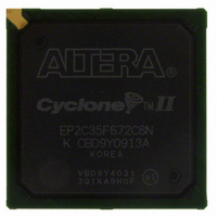
Manufacturer Part Number
EP2C35F672C8N
Description
IC CYCLONE II FPGA 33K 672-FBGA
Manufacturer
Altera
Series
Cyclone® IIr
Datasheet
1.EP2C5T144C8N.pdf
(168 pages)
Specifications of EP2C35F672C8N
Number Of Logic Elements/cells
33216
Number Of Labs/clbs
2076
Total Ram Bits
483840
Number Of I /o
475
Voltage - Supply
1.15 V ~ 1.25 V
Mounting Type
Surface Mount
Operating Temperature
0°C ~ 85°C
Package / Case
672-FBGA
No. Of Logic Blocks
2076
Family Type
Cyclone II
No. Of I/o's
475
I/o Supply Voltage
3.3V
Operating Frequency Max
320MHz
Operating Temperature Range
0°C To +85°C
Rohs Compliant
Yes
For Use With
NANO-CYCLONE - KIT NANOBOARD AND CYCLONEII DC807-1002 - DAUGHTER CARD ALTERA CYCLONE IIP0301 - DE2 CALL FOR ACADEMIC PRICING544-1733 - PCI KIT W/CYCLONE II EP2C35N
Lead Free Status / RoHS Status
Lead free / RoHS Compliant
Number Of Gates
-
Other names
544-1692
Available stocks
Company
Part Number
Manufacturer
Quantity
Price
Company:

Part Number:
EP2C35F672C8N
Manufacturer:
YAGEO
Quantity:
500 000
Company:
Part Number:
EP2C35F672C8N
Manufacturer:
ALTERA
Quantity:
500
Part Number:
EP2C35F672C8N
Manufacturer:
ALTERA/阿尔特拉
Quantity:
20 000


Operating Conditions
5–2
Cyclone II Device Handbook, Volume 1
Notes to
(1)
(2)
(3)
V
V
T
Table 5–2. Recommended Operating Conditions
J
CCINT
CCIO
Symbol
The V
and 2 ms for A devices.
The V
recommended V
specific to the differential standards is given in
The minimum and maximum values of 3.0 V and 3.6 V, respectively, for V
I/O standards. Refer to
(2)
Table
CC
CCIO
must rise monotonically. The maximum V
range given here spans the lowest and highest operating voltages of all supported I/O standards. The
5–2:
Supply voltage for internal
logic and input buffers
Supply voltage for output
buffers, 3.3-V operation
Supply voltage for output
buffers, 2.5-V operation
Supply voltage for output
buffers, 1.8-V operation
Supply voltage for output
buffers, 1.5-V operation
Operating junction
temperature
CCIO
range specific to each of the single-ended I/O standards is given in
Parameter
Table 5–6
Table 5–2
devices. It shows the allowed voltage ranges for V
operating junction temperature (T
powered by V
dedicated clock pins are powered by V
input buffers are powered by both V
for the voltage range of other I/O standards.
specifies the recommended operating conditions for Cyclone II
CCIO
Table
For commercial use
For industrial use
For extended
temperature use
For automotive use
only. The LVDS and LVPECL input buffers on
CC
Conditions
(both V
5–8.
(1)
(1)
(1)
(1)
(1)
CCIO
and V
J
). The LVTTL and LVCMOS inputs are
CCINT
CCINT
3.135 (3.00)
CCINT
Minimum
CCIO
) rise time is 100 ms for non-A devices
2.375
1.425
1.15
1.71
–40
–40
–40
and V
0
only applies to the PCI and PCI-X
. The SSTL, HSTL, LVDS
CCIO
CCINT
Table
.
3.465 (3.60)
Maximum
Altera Corporation
, V
2.625
1.575
1.25
1.89
100
125
125
(3)
85
5–6, and those
CCIO
February 2008
, and the
Unit
°C
°C
°C
°C
V
V
V
V
V
Related parts for EP2C35F672C8N
Image
Part Number
Description
Manufacturer
Datasheet
Request
R

Part Number:
Description:
CYCLONE II STARTER KIT EP2C20N
Manufacturer:
Altera
Datasheet:


Part Number:
Description:
CPLD, EP610 Family, ECMOS Process, 300 Gates, 16 Macro Cells, 16 Reg., 16 User I/Os, 5V Supply, 35 Speed Grade, 24DIP
Manufacturer:
Altera Corporation
Datasheet:
Part Number:
Description:
CPLD, EP610 Family, ECMOS Process, 300 Gates, 16 Macro Cells, 16 Reg., 16 User I/Os, 5V Supply, 15 Speed Grade, 24DIP
Manufacturer:
Altera Corporation
Datasheet:
Part Number:
Description:
Manufacturer:
Altera Corporation
Datasheet:
Part Number:
Description:
CPLD, EP610 Family, ECMOS Process, 300 Gates, 16 Macro Cells, 16 Reg., 16 User I/Os, 5V Supply, 30 Speed Grade, 24DIP
Manufacturer:
Altera Corporation
Datasheet:
Part Number:
Description:
High-performance, low-power erasable programmable logic devices with 8 macrocells, 10ns
Manufacturer:
Altera Corporation
Datasheet:
Part Number:
Description:
High-performance, low-power erasable programmable logic devices with 8 macrocells, 7ns
Manufacturer:
Altera Corporation
Datasheet:
Part Number:
Description:
Classic EPLD
Manufacturer:
Altera Corporation
Datasheet:
Part Number:
Description:
High-performance, low-power erasable programmable logic devices with 8 macrocells, 10ns
Manufacturer:
Altera Corporation
Datasheet:
Part Number:
Description:
Manufacturer:
Altera Corporation
Datasheet:
Part Number:
Description:
Manufacturer:
Altera Corporation
Datasheet:
Part Number:
Description:
Manufacturer:
Altera Corporation
Datasheet:
Part Number:
Description:
CPLD, EP610 Family, ECMOS Process, 300 Gates, 16 Macro Cells, 16 Reg., 16 User I/Os, 5V Supply, 25 Speed Grade, 24DIP
Manufacturer:
Altera Corporation
Datasheet: