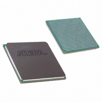
EP2S30F672C5N Altera, EP2S30F672C5N Datasheet - Page 229

EP2S30F672C5N
Manufacturer Part Number
EP2S30F672C5N
Description
IC STRATIX II FPGA 30K 672-FBGA
Manufacturer
Altera
Series
Stratix® IIr
Datasheet
1.EP2S15F484I4N.pdf
(238 pages)
Specifications of EP2S30F672C5N
Number Of Logic Elements/cells
33880
Number Of Labs/clbs
1694
Total Ram Bits
1369728
Number Of I /o
500
Voltage - Supply
1.15 V ~ 1.25 V
Mounting Type
Surface Mount
Operating Temperature
0°C ~ 85°C
Package / Case
672-FBGA
Family Name
Stratix II
Number Of Logic Blocks/elements
33880
# I/os (max)
500
Frequency (max)
609.76MHz
Process Technology
90nm (CMOS)
Operating Supply Voltage (typ)
1.2V
Logic Cells
33880
Ram Bits
1369728
Operating Supply Voltage (min)
1.15V
Operating Supply Voltage (max)
1.25V
Operating Temp Range
0C to 85C
Operating Temperature Classification
Commercial
Mounting
Surface Mount
Pin Count
672
Package Type
FC-FBGA
Family Type
Stratix II
No. Of I/o's
500
I/o Supply Voltage
3.3V
Operating Frequency Max
550MHz
Operating Temperature Range
0°C To +85°C
Logic Case Style
BGA
No. Of Pins
672
Rohs Compliant
Yes
Lead Free Status / RoHS Status
Lead free / RoHS Compliant
Number Of Gates
-
Lead Free Status / Rohs Status
Compliant
Other names
544-1898
EP2S30F672C5N
EP2S30F672C5N
Available stocks
Company
Part Number
Manufacturer
Quantity
Price
Company:
Part Number:
EP2S30F672C5N
Manufacturer:
ALTERA
Quantity:
238
Part Number:
EP2S30F672C5N
Manufacturer:
ALTERA/阿尔特拉
Quantity:
20 000
Altera Corporation
April 2011
Note to
(1)
f
f
f
t
f
f
f
f
t
f
t
t
t
t
I N
I N P F D
I N D U T Y
I N J I T T E R
V C O
O U T
O U T _ I O
S C A N C L K
C O N F I G P L L
C L B W
L O C K
P L L _ P S E R R
A R E S E T
A R E S E T _ R E C O N F I G
Table 5–93. Fast PLL Specifications
Limited by I/O f
Name
Table
5–93:
M A X
Input clock frequency (for -3 and -4 speed
grade devices)
Input clock frequency (for -5 speed grade
devices)
Input frequency to the PFD
Input clock duty cycle
Input clock jitter tolerance in terms of period
jitter. Bandwidth ≤ 2 MHz
Input clock jitter tolerance in terms of period
jitter. Bandwidth > 2 MHz
Upper VCO frequency range for –3 and –4
speed grades
Upper VCO frequency range for –5 speed
grades
Lower VCO frequency range for –3 and –4
speed grades
Lower VCO frequency range for –5 speed
grades
PLL output frequency to
PLL output frequency to LVDS or DPA clock
PLL clock output frequency to regular I/O
pin
Scanclk frequency
Time required to reconfigure scan chains
for fast PLLs
PLL closed-loop bandwidth
Time required for the PLL to lock from the
time it is enabled or the end of the device
configuration
Accuracy of PLL phase shift
Minimum pulse width on
Minimum pulse width on the
when using PLL reconfiguration. Reset the
PLL after
. See
Table 5–77 on page 5–67
scandone
Description
goes high.
GCLK
areset
areset
for the maximum.
or
RCLK
signal.
signal
4.6875
4.6875
16.08
16.08
16.08
1.16
Min
300
300
150
150
150
500
40
10
Stratix II Device Handbook, Volume 1
75/f
DC & Switching Characteristics
S C A N C L K
5.00
0.03
Typ
0.5
1.0
1,040
1,040
28.00
Max
1.00
717
640
500
840
520
420
550
100
±15
(1)
60
ns (p-p)
ns (p-p)
MHz
MHz
MHz
MHz
MHz
MHz
MHz
MHz
MHz
MHz
MHz
MHz
Unit
ms
ns
ps
ns
ns
%
5–93


