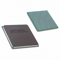
EP2S30F672C5N Altera, EP2S30F672C5N Datasheet - Page 72

EP2S30F672C5N
Manufacturer Part Number
EP2S30F672C5N
Description
IC STRATIX II FPGA 30K 672-FBGA
Manufacturer
Altera
Series
Stratix® IIr
Datasheet
1.EP2S15F484I4N.pdf
(238 pages)
Specifications of EP2S30F672C5N
Number Of Logic Elements/cells
33880
Number Of Labs/clbs
1694
Total Ram Bits
1369728
Number Of I /o
500
Voltage - Supply
1.15 V ~ 1.25 V
Mounting Type
Surface Mount
Operating Temperature
0°C ~ 85°C
Package / Case
672-FBGA
Family Name
Stratix II
Number Of Logic Blocks/elements
33880
# I/os (max)
500
Frequency (max)
609.76MHz
Process Technology
90nm (CMOS)
Operating Supply Voltage (typ)
1.2V
Logic Cells
33880
Ram Bits
1369728
Operating Supply Voltage (min)
1.15V
Operating Supply Voltage (max)
1.25V
Operating Temp Range
0C to 85C
Operating Temperature Classification
Commercial
Mounting
Surface Mount
Pin Count
672
Package Type
FC-FBGA
Family Type
Stratix II
No. Of I/o's
500
I/o Supply Voltage
3.3V
Operating Frequency Max
550MHz
Operating Temperature Range
0°C To +85°C
Logic Case Style
BGA
No. Of Pins
672
Rohs Compliant
Yes
Lead Free Status / RoHS Status
Lead free / RoHS Compliant
Number Of Gates
-
Lead Free Status / Rohs Status
Compliant
Other names
544-1898
EP2S30F672C5N
EP2S30F672C5N
Available stocks
Company
Part Number
Manufacturer
Quantity
Price
Company:
Part Number:
EP2S30F672C5N
Manufacturer:
ALTERA
Quantity:
238
Part Number:
EP2S30F672C5N
Manufacturer:
ALTERA/阿尔特拉
Quantity:
20 000
PLLs & Clock Networks
Figure 2–43. Global & Regional Clock Connections from Top & Bottom Clock Pins & Enhanced PLL Outputs
Notes
Notes to
(1)
(2)
(3)
2–64
Stratix II Device Handbook, Volume 1
EP2S15 and EP2S30 devices only have two enhanced PLLs (5 and 6), but the connectivity from these two PLLs to
the global and regional clock networks remains the same as shown.
If the design uses the feedback input, you lose one (or two, if FBIN is differential) external clock output pin.
The enhanced PLLs can also be driven through the global or regional clock netowrks. The global or regional clock
input can be driven by an output from another PLL, a pin-driven dedicated global or regional clock, or through a
clock control block provided the clock control block is fed by an output from another PLL or a pin-driven dedicated
global or regional clock. An internally generated global signal cannot drive the PLL.
(1), (2), and
Figure
2–43:
(3)
Regional
Regional
Clocks
Clocks
Clocks
Global
RCLK27
RCLK26
RCLK25
RCLK24
RCLK10
RCLK11
RCLK8
RCLK9
c0 c1 c2 c3 c4 c5
c0 c1 c2 c3 c4 c5
PLL 11
PLL 12
c0 c1 c2 c3 c4 c5
c0 c1 c2 c3 c4 c5
PLL 6
PLL 5
RCLK31
RCLK30
RCLK29
RCLK28
G15
G14
G13
G12
G4
G5
G6
G7
RCLK12
RCLK13
RCLK14
RCLK15
Altera Corporation
May 2007


