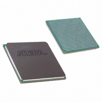
EP2S30F672C5N Altera, EP2S30F672C5N Datasheet - Page 89

EP2S30F672C5N
Manufacturer Part Number
EP2S30F672C5N
Description
IC STRATIX II FPGA 30K 672-FBGA
Manufacturer
Altera
Series
Stratix® IIr
Datasheet
1.EP2S15F484I4N.pdf
(238 pages)
Specifications of EP2S30F672C5N
Number Of Logic Elements/cells
33880
Number Of Labs/clbs
1694
Total Ram Bits
1369728
Number Of I /o
500
Voltage - Supply
1.15 V ~ 1.25 V
Mounting Type
Surface Mount
Operating Temperature
0°C ~ 85°C
Package / Case
672-FBGA
Family Name
Stratix II
Number Of Logic Blocks/elements
33880
# I/os (max)
500
Frequency (max)
609.76MHz
Process Technology
90nm (CMOS)
Operating Supply Voltage (typ)
1.2V
Logic Cells
33880
Ram Bits
1369728
Operating Supply Voltage (min)
1.15V
Operating Supply Voltage (max)
1.25V
Operating Temp Range
0C to 85C
Operating Temperature Classification
Commercial
Mounting
Surface Mount
Pin Count
672
Package Type
FC-FBGA
Family Type
Stratix II
No. Of I/o's
500
I/o Supply Voltage
3.3V
Operating Frequency Max
550MHz
Operating Temperature Range
0°C To +85°C
Logic Case Style
BGA
No. Of Pins
672
Rohs Compliant
Yes
Lead Free Status / RoHS Status
Lead free / RoHS Compliant
Number Of Gates
-
Lead Free Status / Rohs Status
Compliant
Other names
544-1898
EP2S30F672C5N
EP2S30F672C5N
Available stocks
Company
Part Number
Manufacturer
Quantity
Price
Company:
Part Number:
EP2S30F672C5N
Manufacturer:
ALTERA
Quantity:
238
Part Number:
EP2S30F672C5N
Manufacturer:
ALTERA/阿尔特拉
Quantity:
20 000
Figure 2–55. Output TIming Diagram in DDR Mode
Altera Corporation
May 2007
EP2S15
EP2S30
EP2S60
Table 2–14. DQS & DQ Bus Mode Support (Part 1 of 2)
Device
From Internal
484-pin FineLine BGA
672-pin FineLine BGA
484-pin FineLine BGA
672-pin FineLine BGA
484-pin FineLine BGA
672-pin FineLine BGA
1,020-pin FineLine BGA
Registers
DDR output
Package
CLK
The Stratix II IOE operates in bidirectional DDR mode by combining the
DDR input and DDR output configurations. The negative-edge-clocked
OE register holds the OE signal inactive until the falling edge of the clock.
This is done to meet DDR SDRAM timing requirements.
External RAM Interfacing
In addition to the six I/O registers in each IOE, Stratix II devices also have
dedicated phase-shift circuitry for interfacing with external memory
interfaces. Stratix II devices support DDR and DDR2 SDRAM, QDR II
SRAM, RLDRAM II, and SDR SDRAM memory interfaces. In every
Stratix II device, the I/O banks at the top (banks 3 and 4) and bottom
(banks 7 and 8) of the device support DQ and DQS signals with DQ bus
modes of ×4, ×8/×9, ×16/×18, or ×32/×36.
of DQ and DQS buses that are supported per device.
A1
B1
B1
A1
Number of
×4 Groups
B2
A2
B2
18
18
18
36
8
8
8
A2
A3
B3
B3
×8/×9 Groups
Number of
Note (1)
A3
18
4
8
4
8
4
8
A4
B4
B4
Stratix II Device Handbook, Volume 1
A4
×16/×18 Groups
Table 2–14
Number of
0
4
0
4
0
4
8
Stratix II Architecture
shows the number
×32/×36 Groups
Number of
0
0
0
0
0
0
4
2–81


