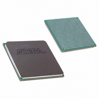
EP1SGX10DF672I6 Altera, EP1SGX10DF672I6 Datasheet - Page 182

EP1SGX10DF672I6
Manufacturer Part Number
EP1SGX10DF672I6
Description
IC STRATIX GX FPGA 10KLE 672FBGA
Manufacturer
Altera
Series
Stratix® GXr
Datasheet
1.EP1SGX10CF672C7N.pdf
(272 pages)
Specifications of EP1SGX10DF672I6
Number Of Logic Elements/cells
10570
Number Of Labs/clbs
1057
Total Ram Bits
920448
Number Of I /o
362
Voltage - Supply
1.425 V ~ 1.575 V
Mounting Type
Surface Mount
Operating Temperature
-40°C ~ 100°C
Package / Case
672-FBGA
Family Name
Stratix GX
Number Of Logic Blocks/elements
10570
# I/os (max)
362
Frequency (max)
5GHz
Process Technology
SRAM
Operating Supply Voltage (typ)
1.5V
Logic Cells
10570
Ram Bits
920448
Operating Supply Voltage (min)
1.425V
Operating Supply Voltage (max)
1.575V
Operating Temp Range
-40C to 100C
Operating Temperature Classification
Industrial
Mounting
Surface Mount
Pin Count
672
Package Type
FC-FBGA
Lead Free Status / RoHS Status
Contains lead / RoHS non-compliant
Number Of Gates
-
Lead Free Status / Rohs Status
Not Compliant
Available stocks
Company
Part Number
Manufacturer
Quantity
Price
- Current page: 182 of 272
- Download datasheet (3Mb)
I/O Structure
Figure 4–69. Stratix GX I/O Banks
Notes to
(1)
(2)
(3)
(4)
(5)
4–116
Stratix GX Device Handbook, Volume 1
PLL8
PLL7
PLL1
PLL2
Figure 4–69
Banks 9 through 12 are enhanced PLL external clock output banks.
If the high-speed differential I/O pins are not used for high-speed differential signaling, they can support all of the
I/O standards except HSTL class I and II, GTL, SSTL-18 Class II, PCI, PCI-X, and AGP 1×/2×.
For guidelines for placing single-ended I/O pads next to differential I/O pads, see the Selectable I/O Standards in
Stratix & Stratix GX Devices chapter in the Stratix GX Device Handbook, Volume 2.
These I/O banks in Stratix GX devices also support the LVDS, LVPECL, and 3.3-V PCML I/O standards on reference
clocks and receiver input pins (AC coupled)
VREF1B3 VREF2B3 VREF3B3 VREF4B3 VREF5B3
VREF5B8 VREF4B8 VREF3B8 VREF2B8 VREF1B8
DQST9
DQSB9
(4)
(4)
Figure
DQST8
DQSB8
and HyperTransport I/O Block
LVDS, LVPECL, 3.3-V PCML,
and HyperTransport I/O Block
and Regular I/O Pins
LVDS, LVPECL, 3.3-V PCML,
4–69:
is a top view of the Stratix GX silicon die.
and Regular I/O Pins
DQST7
DQSB7
Bank 8
Bank 3
I/O Banks 1 and 2 Support All
Single-Ended I/O Standards Except
Differential HSTL Output Clocks,
Differential SSTL-2 Output Clocks,
HSTL Class II, GTL, SSTL-18 Class II,
PCI, PCI-X, and AGP 1×/2×
DQSB6
DQST6
(3)
(3)
DQSB5
DQST5
I/O Banks 3, 4, 9 & 10 Support
All Single-Ended I/O Standards
I/O Banks 7, 8, 11 & 12 Support
All Single-Ended I/O Standards
Notes
11
9
PLL5
PLL6
(1), (2),
10
12
PLL11
PLL12
(3)
VREF1B4 VREF2B4 VREF3B4 VREF4B4 VREF5B4
VREF5B7 VREF4B7 VREF3B7 VREF2B7 VREF1B7
DQST4
DQSB4
(2)
1.5-V PCML
(2)
DQST3
DQSB3
(5)
DQSB2
DQST2
Bank 7
Bank 4
DQST1
DQSB1
DQST0
DQSB0
Altera Corporation
February 2005
I/O Bank 13
I/O Bank 14
I/O Bank 17
I/O Bank 16
I/O Bank 15
(5)
(5)
(5)
(5)
(5)
Related parts for EP1SGX10DF672I6
Image
Part Number
Description
Manufacturer
Datasheet
Request
R

Part Number:
Description:
CYCLONE II STARTER KIT EP2C20N
Manufacturer:
Altera
Datasheet:

Part Number:
Description:
CPLD, EP610 Family, ECMOS Process, 300 Gates, 16 Macro Cells, 16 Reg., 16 User I/Os, 5V Supply, 35 Speed Grade, 24DIP
Manufacturer:
Altera Corporation
Datasheet:

Part Number:
Description:
CPLD, EP610 Family, ECMOS Process, 300 Gates, 16 Macro Cells, 16 Reg., 16 User I/Os, 5V Supply, 15 Speed Grade, 24DIP
Manufacturer:
Altera Corporation
Datasheet:

Part Number:
Description:
Manufacturer:
Altera Corporation
Datasheet:

Part Number:
Description:
CPLD, EP610 Family, ECMOS Process, 300 Gates, 16 Macro Cells, 16 Reg., 16 User I/Os, 5V Supply, 30 Speed Grade, 24DIP
Manufacturer:
Altera Corporation
Datasheet:

Part Number:
Description:
High-performance, low-power erasable programmable logic devices with 8 macrocells, 10ns
Manufacturer:
Altera Corporation
Datasheet:

Part Number:
Description:
High-performance, low-power erasable programmable logic devices with 8 macrocells, 7ns
Manufacturer:
Altera Corporation
Datasheet:

Part Number:
Description:
Classic EPLD
Manufacturer:
Altera Corporation
Datasheet:

Part Number:
Description:
High-performance, low-power erasable programmable logic devices with 8 macrocells, 10ns
Manufacturer:
Altera Corporation
Datasheet:

Part Number:
Description:
Manufacturer:
Altera Corporation
Datasheet:

Part Number:
Description:
Manufacturer:
Altera Corporation
Datasheet:

Part Number:
Description:
Manufacturer:
Altera Corporation
Datasheet:

Part Number:
Description:
CPLD, EP610 Family, ECMOS Process, 300 Gates, 16 Macro Cells, 16 Reg., 16 User I/Os, 5V Supply, 25 Speed Grade, 24DIP
Manufacturer:
Altera Corporation
Datasheet:


