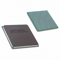
EP1SGX10DF672I6 Altera, EP1SGX10DF672I6 Datasheet - Page 237

EP1SGX10DF672I6
Manufacturer Part Number
EP1SGX10DF672I6
Description
IC STRATIX GX FPGA 10KLE 672FBGA
Manufacturer
Altera
Series
Stratix® GXr
Datasheet
1.EP1SGX10CF672C7N.pdf
(272 pages)
Specifications of EP1SGX10DF672I6
Number Of Logic Elements/cells
10570
Number Of Labs/clbs
1057
Total Ram Bits
920448
Number Of I /o
362
Voltage - Supply
1.425 V ~ 1.575 V
Mounting Type
Surface Mount
Operating Temperature
-40°C ~ 100°C
Package / Case
672-FBGA
Family Name
Stratix GX
Number Of Logic Blocks/elements
10570
# I/os (max)
362
Frequency (max)
5GHz
Process Technology
SRAM
Operating Supply Voltage (typ)
1.5V
Logic Cells
10570
Ram Bits
920448
Operating Supply Voltage (min)
1.425V
Operating Supply Voltage (max)
1.575V
Operating Temp Range
-40C to 100C
Operating Temperature Classification
Industrial
Mounting
Surface Mount
Pin Count
672
Package Type
FC-FBGA
Lead Free Status / RoHS Status
Contains lead / RoHS non-compliant
Number Of Gates
-
Lead Free Status / Rohs Status
Not Compliant
Available stocks
Company
Part Number
Manufacturer
Quantity
Price
- Current page: 237 of 272
- Download datasheet (3Mb)
Altera Corporation
June 2006
Notes to
(1)
(2)
(3)
(4)
(5)
t
t
t
t
t
A N A L O G R E S E T P W
D I G I TA L R E S E T P W
T X _ P L L _ L O C K
R X _ F R E Q L O C K
R X _ F R E Q L O C K 2 P H A S E L O C K
Table 6–50. Stratix GX Transceiver Reset & PLL Lock Time Parameters
The minimum pulse width specified is associated with the power-down of circuits.
The clock recovery unit (CRU) phase locked-to-data time is based on a data rate of 500 Mbps and 8B/10B encoded
data.
After
reference clock.
After
There is no maximum pulse width specification. The GXB can be held in reset indefinitely.
Table
#pll_areset
#rx_analogreset
Symbol
(3)
6–50:
(4)
(5)
(5)
,
pll_enable
(2)
Routing delays vary depending on the load on a specific routing line. The
Quartus II software reports the routing delay information when running
the timing analysis for a design. Contact Altera Applications Engineering
for more details.
External Timing Parameters
External timing parameters are specified by device density and speed
grade.
timing. All registers are within the IOE.
, the time for the CRU to switch to lock-to-data mode.
Figure 6–6
Min
, or PLL power-up, the time required for the transceiver PLL to lock to the
1
4
shows the timing model for bidirectional IOE pin
Typ
Stratix GX Device Handbook, Volume 1
DC & Switching Characteristics
Max
10
5
5
mS
Parallel clock
cycle
µS
mS
µS
Units
6–35
Related parts for EP1SGX10DF672I6
Image
Part Number
Description
Manufacturer
Datasheet
Request
R

Part Number:
Description:
CYCLONE II STARTER KIT EP2C20N
Manufacturer:
Altera
Datasheet:

Part Number:
Description:
CPLD, EP610 Family, ECMOS Process, 300 Gates, 16 Macro Cells, 16 Reg., 16 User I/Os, 5V Supply, 35 Speed Grade, 24DIP
Manufacturer:
Altera Corporation
Datasheet:

Part Number:
Description:
CPLD, EP610 Family, ECMOS Process, 300 Gates, 16 Macro Cells, 16 Reg., 16 User I/Os, 5V Supply, 15 Speed Grade, 24DIP
Manufacturer:
Altera Corporation
Datasheet:

Part Number:
Description:
Manufacturer:
Altera Corporation
Datasheet:

Part Number:
Description:
CPLD, EP610 Family, ECMOS Process, 300 Gates, 16 Macro Cells, 16 Reg., 16 User I/Os, 5V Supply, 30 Speed Grade, 24DIP
Manufacturer:
Altera Corporation
Datasheet:

Part Number:
Description:
High-performance, low-power erasable programmable logic devices with 8 macrocells, 10ns
Manufacturer:
Altera Corporation
Datasheet:

Part Number:
Description:
High-performance, low-power erasable programmable logic devices with 8 macrocells, 7ns
Manufacturer:
Altera Corporation
Datasheet:

Part Number:
Description:
Classic EPLD
Manufacturer:
Altera Corporation
Datasheet:

Part Number:
Description:
High-performance, low-power erasable programmable logic devices with 8 macrocells, 10ns
Manufacturer:
Altera Corporation
Datasheet:

Part Number:
Description:
Manufacturer:
Altera Corporation
Datasheet:

Part Number:
Description:
Manufacturer:
Altera Corporation
Datasheet:

Part Number:
Description:
Manufacturer:
Altera Corporation
Datasheet:

Part Number:
Description:
CPLD, EP610 Family, ECMOS Process, 300 Gates, 16 Macro Cells, 16 Reg., 16 User I/Os, 5V Supply, 25 Speed Grade, 24DIP
Manufacturer:
Altera Corporation
Datasheet:


