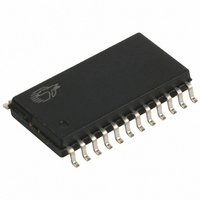
CY7C63743-SXC Cypress Semiconductor Corp, CY7C63743-SXC Datasheet - Page 22

CY7C63743-SXC
Manufacturer Part Number
CY7C63743-SXC
Description
IC MCU 8K USB/PS2 LS 24SOIC
Manufacturer
Cypress Semiconductor Corp
Series
enCoRe™r
Specifications of CY7C63743-SXC
Applications
USB Microcontroller
Core Processor
M8B
Program Memory Type
OTP (8 kB)
Controller Series
CY7C637xx
Ram Size
256 x 8
Interface
PS2, USB
Number Of I /o
16
Voltage - Supply
4 V ~ 5.5 V
Operating Temperature
0°C ~ 70°C
Mounting Type
Surface Mount
Package / Case
24-SOIC (7.5mm Width)
Lead Free Status / RoHS Status
Lead free / RoHS Compliant
Other names
428-1622
Available stocks
Company
Part Number
Manufacturer
Quantity
Price
Part Number:
CY7C63743-SXC
Manufacturer:
CYPRESS/赛普拉斯
Quantity:
20 000
Serial Peripheral Interface (SPI)
SPI is a four-wire, full-duplex serial communication interface
between a master device and one or more slave devices. The
CY7C637xxC SPI circuit supports byte serial transfers in either
Master or Slave modes. The block diagram of the SPI circuit is
shown in
and receive data for maximum flexibility and throughput. The
The SPI Data Register below serves as a transmit and receive
buffer.
Figure 21. SPI Data Register (Address 0x60)
Bit [7:0]: Data I/O[7:0]
Operation as an SPI Master
Only an SPI Master can initiate a byte/data transfer. This is done
by the Master writing to the SPI Data Register. The Master shifts
out 8 bits of data (MSB first) along with the serial clock SCK for
the Slave. The Master’s outgoing byte is replaced with an
incoming one from a Slave device. When the last bit is received,
the shift register contents are transferred to the receive buffer
and an interrupt is generated. The receive data must be read
Document #: 38-08022 Rev. *D
Read/Write R/W R/W R/W R/W R/W R/W R/W R/W
Bit Name
Writes to the SPI Data Register load the transmit buffer, while
reads from this register read the receive buffer contents.
1 = Logic HIGH
0 = Logic LOW
Reset
Bit #
Figure
20. The block contains buffers for both transmit
7
0
6
0
5
0
Data I/O
4
0
Data Bus
3
0
8 bit shift register
Data Bus
RX Buffer
TX Buffer
2
0
Figure 20. SPI Block Diagram
1
0
Write
Read
0
0
CY7C637xxC can be configured as either an SPI Master or
Slave. The external interface consists of Master-Out/Slave-In
(MOSI), Master-In/Slave-Out (MISO), Serial Clock (SCK), and
Slave Select (SS).
SPI modes are activated by setting the appropriate bits in the SPI
Control Register, as described below.
from the SPI Data Register before the next byte of data is trans-
ferred to the receive buffer, or the data will be lost.
When operating as a Master, an active LOW Slave Select (SS)
must be generated to enable a Slave for a byte transfer. This
Slave Select is generated under firmware control, and is not part
of the SPI internal hardware. Any available GPIO can be used
for the Master’s Slave Select output.
When the Master writes to the SPI Data Register, the data is
loaded into the transmit buffer. If the shift register is not busy
shifting a previous byte, the TX buffer contents will be automati-
cally transferred into the shift register and shifting will begin. If
the shift register is busy, the new byte will be loaded into the shift
register only after the active byte has finished and is transferred
to the receive buffer. The new byte will then be shifted out. The
Transmit Buffer Full (TBF) bit will be set HIGH until the transmit
buffer’s data-byte is transferred to the shift register. Writing to the
transmit buffer while the TBF bit is HIGH will overwrite the old
byte in the transmit buffer.
The byte shifting and SCK generation are handled by the
hardware (based on firmware selection of the clock source).
Data is shifted out on the MOSI pin (P0.5) and the serial clock is
output on the SCK pin (P0.7). Data is received from the slave on
the MISO pin (P0.6). The output pins must be set to the desired
drive strength, and the GPIO data register must be set to 1 to
enable a bypass mode for these pins. The MISO pin must be
configured in the desired GPIO input mode. See Section for
GPIO configuration details.
Internal SCK
Master
/ Slave
Control
4
MOSI
MISO
SCK
SS
CY7C63722C
CY7C63723C
CY7C63743C
Page 22 of 53
[+] Feedback


