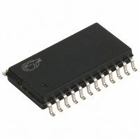
CY7C63743-SXC Cypress Semiconductor Corp, CY7C63743-SXC Datasheet - Page 37

CY7C63743-SXC
Manufacturer Part Number
CY7C63743-SXC
Description
IC MCU 8K USB/PS2 LS 24SOIC
Manufacturer
Cypress Semiconductor Corp
Series
enCoRe™r
Specifications of CY7C63743-SXC
Applications
USB Microcontroller
Core Processor
M8B
Program Memory Type
OTP (8 kB)
Controller Series
CY7C637xx
Ram Size
256 x 8
Interface
PS2, USB
Number Of I /o
16
Voltage - Supply
4 V ~ 5.5 V
Operating Temperature
0°C ~ 70°C
Mounting Type
Surface Mount
Package / Case
24-SOIC (7.5mm Width)
Lead Free Status / RoHS Status
Lead free / RoHS Compliant
Other names
428-1622
Available stocks
Company
Part Number
Manufacturer
Quantity
Price
Part Number:
CY7C63743-SXC
Manufacturer:
CYPRESS/赛普拉斯
Quantity:
20 000
The response of the SIE can be summarized as follows:
Table 10. Details of Modes for Differing Traffic Conditions
Document #: 38-08022 Rev. *D
1. The SIE will only respond to valid transactions, and will ignore
2. The SIE will generate an interrupt when a valid transaction is
3. An incoming Data packet is valid if the count is < Endpoint
4. An IN will be ignored by an OUT configured endpoint and visa
5. The IN and OUT PID status is updated at the end of a trans-
End Point Mode
3
SETUP Packet
See8
See8
See 8
Disabled
0
NAK IN/OUT
0
0
0
0
Ignore IN/OUT
0
0
STALL IN/OUT
0
0
0
0
Control Write
ACK OUT/NAK IN
1
1
1
non-valid ones.
completed or when the FIFO is corrupted. FIFO corruption
occurs during an OUT or SETUP transaction to a valid internal
address, that ends with a non-valid CRC.
Size + 2 (includes CRC) and passes all error checking;
versa.
action.
2
0
0
0
0
0
1
1
0
0
0
0
0
0
0
1
0
0
0
0
0
0
0
1
1
1
1
1
1
1
0 x
1 OUT
1 OUT
1 IN
1 OUT
1 OUT
1 IN
1 OUT
0
1 OUT
0 OUT
0 IN
1 OUT
1 OUT
1 OUT
Rcved
Token
SETUP
SETUP
SETUP
(if accepting)
Cou
nt
<=
10
> 10
x
x
x
> 10
x
x
x
x
x
> 10
x
x
<=
10
> 10
x
Buffer
data
junk
junk
UC
UC
UC
UC
UC
UC
UC
UC
UC
UC
UC
data
junk
junk
Dval
valid
x
invalid
x
x
x
invalid
x
x
x
x
x
invalid
x
valid
x
invalid
DTOG
up-
dates
up-
dates
up-
dates
UC
UC
UC
UC
UC
UC
UC
UC
UC
UC
UC
up-
dates
up-
dates
up-
dates
DVAL
1
up-
dates
0
UC
UC
UC
UC
UC
UC
UC
UC
UC
UC
UC
1
up-
dates
0
COUN
T
up-
dates
up-
dates
up-
dates
UC
UC
UC
UC
UC
UC
UC
UC
UC
UC
UC
up-
dates
up-
dates
up-
dates
6. The SETUP PID status is updated at the beginning of the Data
7. The entire Endpoint 0 mode register and the Count register
packet phase.
are locked to CPU writes at the end of any transaction to that
endpoint in which an ACK is transferred. These registers are
only unlocked by a CPU read of these registers, and only if
that read happens after the transaction completes. This repre-
sents about a 1-μs window in which the CPU is locked from
register writes to these USB registers. Normally the firmware
should perform a register read at the beginning of the
Endpoint ISRs to unlock and get the mode register infor-
mation. The interlock on the Mode and Count registers
ensures that the firmware recognizes the changes that the
SIE might have made during the previous transaction.
SET-
UP
1
1
UC
UC
UC
UC
UC
UC
UC
UC
UC
UC
UC
UC
UC
PID
1
UC
IN
U
C
U
C
U
C
U
C
U
C
U
C
U
C
1
U
C
U
C
U
C
U
C
U
C
1
U
C
U
C
U
C
OU
T
UC
UC
UC
UC
1
UC
UC
UC
UC
UC
1
UC
UC
UC
1
1
1
ACK
1
UC
UC
UC
UC
UC
UC
UC
UC
UC
UC
UC
UC
UC
1
UC
UC
Set End Point Mode
3
0
NoChang
e
NoChang
e
NoChang
e
NoChang
e
NoChang
e
NoChang
e
NoChang
e
NoChang
e
NoChang
e
NoChang
e
NoChang
e
NoChang
e
NoChang
e
0
NoChang
e
NoChang
e
2 1 0 Response
0 0 1 ACK
0 0 1 ACK
CY7C63722C
CY7C63723C
CY7C63743C
Ignore
Ignore
Ignore
NAK
Ignore
Ignore
NAK
Ignore
Ignore
STALL
Ignore
Ignore
STALL
Ignore
Ignore
Page 37 of 53
Int
ye
s
ye
s
ye
s
no
ye
s
no
no
ye
s
no
no
ye
s
no
no
ye
s
ye
s
ye
s
ye
s
[+] Feedback


