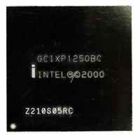
GCIXP1250BC Intel, GCIXP1250BC Datasheet - Page 14

GCIXP1250BC
Manufacturer Part Number
GCIXP1250BC
Description
IC MPU NETWORK 232MHZ 520-BGA
Manufacturer
Intel
Specifications of GCIXP1250BC
Rohs Status
RoHS non-compliant
Processor Type
Network
Features
32-bit StrongARM RISC Core
Speed
232MHz
Voltage
3.3V
Mounting Type
Surface Mount
Package / Case
520-BGA
Pin Count
520
Mounting
Surface Mount
Operating Temperature (max)
85C
Operating Temperature (min)
-40C
Operating Temperature Classification
Industrial
Lead Free Status / Rohs Status
Not Compliant
Other names
837414
Available stocks
Company
Part Number
Manufacturer
Quantity
Price
Company:
Part Number:
GCIXP1250BC
Manufacturer:
INTEL
Quantity:
77
Intel
Errata
Workaround:
14
®
IXP1250 Network Processor
Note: Great care must be taken to ensure that different optional tokens are carried over to the workaround
For example, if the thread waits for the completion of the write_unlock command that gets dropped
(either using the ctx_swap optional token, or, the sig_done optional token and ctx_arb[SRAM]
command), then that thread will hang indefinitely. Further, the write to the memory location will
not complete leading to data corruption problems. And, because a different command gets executed
twice, two SRAM signals may be generated to a different thread, leading to improper program flow
and data corruption.
It is recommended that the software programs not use the SRAM[WRITE_UNLOCK,…,ref_cnt]
command with a ref_cnt > 1. If more than one long word needs to be written to memory, the
software should use the workarounds described below.
Two workarounds have been developed and are described below:
Workaround 1 requires two Microengine Instruction Control Store locations, but results in one
extra SRAM bus write cycle. It is possible to eliminate the extra bus cycle by suitably modifying
the transfer register, address, and, ref_cnt fields, but may result extra Microengine instructions
needed to compute the address. A simple case is illustrated in the examples below for this.
Workaround 2 does not have the extra bus access but may require a third ctx_arb[SRAM]
instruction if the program needs to wait for completion of the command. Examples shown below
will illustrate this point.
to ensure correct program flow. The examples below are given to illustrate some key
considerations.
Example A – No optional tokens.
Original code
SRAM[WRITE_UNLOCK, $x1, sAddr, 0, 3]
Workaround 1
SRAM[WRITE, $x2, sAddr, 1, 2]
SRAM[WRITE_UNLOCK, $x1, sAddr, 0, 1]
Workaround 2
SRAM[WRITE, $x1, sAddr, 0, 3]
SRAM[UNLOCK, --, sAddr, 0, 1]
Example B – CTX_SWAP optional token.
Original code
SRAM[WRITE_UNLOCK, $x1, sAddr, 0, 3], ctx_swap
Workaround 1
SRAM[WRITE, $x2, sAddr,1, 2]
SRAM[WRITE_UNLOCK, $x1, sAddr, 0, 1],ctx_swap
Workaround 2
SRAM[WRITE, $x1, sAddr, 0, 3], sig_done
SRAM[UNLOCK, --, sAddr, 0, 1]
1. Break the SRAM[WRITE_UNLOCK,..., ref_cnt] instruction into a SRAM[write, …, ref_cnt]
2. Break the SRAM[WRITE_UNLOCK,....], instruction into a SRAM[write, …, ref_cnt] and
and SRAM[WRITE_UNLOCK,..., 1] pair.
SRAM[UNLOCK,..., 1] pair.
Specification Update


