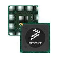
MPC8313VRADDB Freescale Semiconductor, MPC8313VRADDB Datasheet - Page 10

MPC8313VRADDB
Manufacturer Part Number
MPC8313VRADDB
Description
MPU POWERQUICC II PRO 516-PBGA
Manufacturer
Freescale Semiconductor
Datasheet
1.MPC8313CZQAFFB.pdf
(100 pages)
Specifications of MPC8313VRADDB
Processor Type
MPC83xx PowerQUICC II Pro 32-Bit
Speed
267MHz
Voltage
0.95 V ~ 1.05 V
Mounting Type
Surface Mount
Package / Case
516-PBGA
Processor Series
MPC8xxx
Core
e300
Data Bus Width
32 bit
Development Tools By Supplier
MPC8313E-RDB
Maximum Clock Frequency
400 MHz
Operating Supply Voltage
- 0.3 V to + 1.26 V
Maximum Operating Temperature
+ 105 C
Mounting Style
SMD/SMT
Data Ram Size
16 KB
I/o Voltage
2.5 V
Interface Type
I2C, SPI, UART
Minimum Operating Temperature
- 40 C
Program Memory Type
EEPROM/Flash
Lead Free Status / RoHS Status
Lead free / RoHS Compliant
Features
-
Lead Free Status / Rohs Status
Lead free / RoHS Compliant
Available stocks
Company
Part Number
Manufacturer
Quantity
Price
Company:
Part Number:
MPC8313VRADDB
Manufacturer:
MOTOLOLA
Quantity:
885
Company:
Part Number:
MPC8313VRADDB
Manufacturer:
Freescale Semiconductor
Quantity:
10 000
Power Characteristics
and V
supplies fully ramp up. In the case where the core voltage is applied first, the core voltage supply must rise
to 90% of its nominal value before the I/O supplies reach 0.7 V; see
(I/O voltage and core voltage) are stable, wait for a minimum of 32 clock cycles before negating
PORESET.
Note that there is no specific power down sequence requirement for the MPC8313E. I/O voltage supplies
(GV
3
The estimated typical power dissipation, not including I/O supply power, for this family of MPC8313E
devices is shown in
10
DD
DDC
, LV
Power Characteristics
1
2
3
Core Frequency
The values do not include I/O supply power or AV
digital power (not including XCOREV
the SerDes PHY).
Typical power is based on a voltage of V
temperature.
Maximum power is based on a voltage of V
smoker test.
) before the I/O voltage (GV
DD
(MHz)
, and OV
333
400
90%
MPC8313E PowerQUICC
Table
V
0
DD
PORESET
4.
) do not have any ordering requirements with respect to one another.
CSB Frequency
Table 5
(MHz)
Figure 3. Power-Up Sequencing Example
167
133
Table 4. MPC8313E Power Dissipation
shows the estimated typical I/O power dissipation.
DD
DD
™
, LV
, XPADV
II Pro Processor Hardware Specifications, Rev. 3
DD
DD
= 1.05 V and an artificial smoker test running at room
Typical
DD
= 1.05 V, a junction temperature of T
820
820
DD
, and OV
DD
, or SDAV
, but do include core, USB PLL, and a portion of SerDes
2
I/O Voltage (GV
t
SYS_CLK_IN
Maximum for
DD
DD
Silicon
Rev. 1.0
, which all have dedicated power supplies for
) and assert PORESET before the power
1020
1020
Core Voltage (V
/t
3
PCI_SYNC_IN
Figure
DD
, GV
1
Rev. 2.x or Later
3. Once both the power supplies
Maximum for
DD
DD
, and OV
Silicon
J
>= 32 clocks
= 105°C, and an artificial
1200
1200
, V
0.7 V
DDC
3
)
DD
Freescale Semiconductor
)
t
Unit
mW
mW


