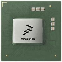
MPC8541EVTAQF Freescale Semiconductor, MPC8541EVTAQF Datasheet - Page 49

MPC8541EVTAQF
Manufacturer Part Number
MPC8541EVTAQF
Description
IC MPU POWERQUICC III 783-FCPBGA
Manufacturer
Freescale Semiconductor
Datasheet
1.MPC8541EVTALF.pdf
(88 pages)
Specifications of MPC8541EVTAQF
Processor Type
MPC85xx PowerQUICC III 32-Bit
Speed
1.0GHz
Voltage
1.3V
Mounting Type
Surface Mount
Package / Case
783-FCPBGA
Processor Series
MPC85xx
Core
e500
Data Bus Width
32 bit
Development Tools By Supplier
RDK-IDM-SBC
Maximum Clock Frequency
1000 MHz
Maximum Operating Temperature
+ 105 C
Mounting Style
SMD/SMT
I/o Voltage
2.5 V, 3.3 V
Minimum Operating Temperature
0 C
For Use With
MPC8548CDS - DEV TOOLS CDS FOR 8548CWH-PPC-8540N-VE - KIT EVAL SYSTEM MPC8540
Lead Free Status / RoHS Status
Lead free / RoHS Compliant
Features
-
Lead Free Status / Rohs Status
Lead free / RoHS Compliant
Available stocks
Company
Part Number
Manufacturer
Quantity
Price
Company:
Part Number:
MPC8541EVTAQF
Manufacturer:
Freescale Semiconductor
Quantity:
10 000
Figure 31
Figure 32
Figure 33
Figure 34
Freescale Semiconductor
MPC8541E PowerQUICC™ III Integrated Communications Processor Hardware Specification, Rev. 4.2
provides the AC test load for TDO and the boundary-scan outputs of the MPC8541E.
provides the JTAG clock input timing diagram.
provides the TRST timing diagram.
provides the boundary-scan timing diagram.
External Clock
Data Outputs
Data Outputs
Data Inputs
External Clock
Boundary
Boundary
Boundary
TRST
JTAG
JTAG
Output
t
Output Data Valid
JTKLDX
Figure 31. AC Test Load for the JTAG Interface
Figure 32. JTAG Clock Input Timing Diagram
Figure 34. Boundary-Scan Timing Diagram
VM
t
JTKHKL
Figure 33. TRST Timing Diagram
VM
t
Z
VM
JTKLDZ
VM = Midpoint Voltage (OV DD /2)
VM = Midpoint Voltage (OV DD /2)
VM = Midpoint Voltage (OV DD /2)
t
0
JTKLDV
t
= 50 Ω
JTG
VM
t
TRST
t
JTDVKH
VM
R
VM
Output Data Valid
L
Data Valid
= 50 Ω
Input
t
JTGR
VM
OV
DD
t
t
JTDXKH
JTGF
/2
JTAG
49


