TDA8023TT/C1,118 NXP Semiconductors, TDA8023TT/C1,118 Datasheet - Page 13

TDA8023TT/C1,118
Manufacturer Part Number
TDA8023TT/C1,118
Description
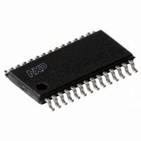
IC SMART CARD INTERFACE 28-TSSOP
Manufacturer
NXP Semiconductors
Datasheet
1.TDA8023TTC1118.pdf
(32 pages)
Specifications of TDA8023TT/C1,118
Package / Case
28-TSSOP
Controller Type
Smart Card Interface
Interface
I²C
Voltage - Supply
2.7 V ~ 6.5 V
Current - Supply
200mA
Operating Temperature
-40°C ~ 85°C
Mounting Type
Surface Mount
Maximum Operating Temperature
+ 85 C
Minimum Operating Temperature
- 40 C
Mounting Style
SMD/SMT
Lead Free Status / RoHS Status
Lead free / RoHS Compliant
Lead Free Status / RoHS Status
Lead free / RoHS Compliant, Lead free / RoHS Compliant
Other names
935274975118
TDA8023TT-T
TDA8023TT-T
TDA8023TT-T
TDA8023TT-T
NXP Semiconductors
TDA8023_1
Product data sheet
8.4.2 Inductive configuration
8.6.1 Activation sequence
8.5 V
8.6 Sequencer and clock counter
The external components are a diode, a coil of 6.8 H and a capacitor of 4.7 F (see
Figure
In all modes (follower, doubler, tripler), the DC-to-DC converter is able to deliver 60 mA
over the whole V
The current on the V
reached, an automatic deactivation sequence is performed.
The V
168 nF. If the card socket is not very close to the TDA8023, one capacitor should be
placed near the TDA8023, and a second one near the card contacts.
The sequencer takes care of ensuring activation and deactivation sequences according to
ISO 7816 and EMV 2000, even in case of emergency (card removal during transaction,
supply dropout or hardware problem).
The sequencer is clocked with an internal oscillator.
The activation of a card is initiated by setting bit START in the Command register, which is
only possible if the card is present and if the voltage supervisor is not active. The
activation sequence is described in
The deactivation is initiated either by the system controller or automatically in case of a
hardware problem or a supply dropout. The deactivation sequence is described in
Section
Outside a session, card contacts are forced low-impedance with respect to pin GNDC.
When the card is inactive, pins V
with respect to pin GNDC. The DC-to-DC converter is stopped.
•
•
•
•
•
CC
Doubler:
– If V
– If V
Tripler:
– If V
If V
If V
If V
buffer
CC
2). In this configuration the DC-to-DC converter acts as follows.
CC
CC
CC
8.6.2.
voltage should be decoupled with a low-ESR capacitor between 100 nF and
CC
CC
CC
= 5 V then V
= 3 V then V
= 1.8 V then the DC-to-DC converter acts as a follower
= 5 V and V
= 3 V and V
= 5 V and V
DD
range (2.7 V to 6.5 V) or 90 mA if V
CC
VUP
VUP
buffer has an internal limitation of around 90 mA. When this limit is
Rev. 01 — 16 July 2007
DD(DCDC)
DD(DCDC)
DD(DCDC)
is regulated at 5.5 V
is regulated at 4 V
CC
= 4 V to 5.8 V
< 4 V
< 4 V
, CLK, RST and I/O are LOW, which is low-impedance
Section
8.6.1.
DD
> 3 V.
Low power IC card interface
TDA8023
© NXP B.V. 2007. All rights reserved.
13 of 32


