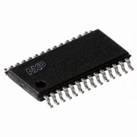
TDA8023TT/C1,118 NXP Semiconductors, TDA8023TT/C1,118 Datasheet - Page 20

TDA8023TT/C1,118
Manufacturer Part Number
TDA8023TT/C1,118
Description
IC SMART CARD INTERFACE 28-TSSOP
Manufacturer
NXP Semiconductors
Datasheet
1.TDA8023TTC1118.pdf
(32 pages)
Specifications of TDA8023TT/C1,118
Package / Case
28-TSSOP
Controller Type
Smart Card Interface
Interface
I²C
Voltage - Supply
2.7 V ~ 6.5 V
Current - Supply
200mA
Operating Temperature
-40°C ~ 85°C
Mounting Type
Surface Mount
Maximum Operating Temperature
+ 85 C
Minimum Operating Temperature
- 40 C
Mounting Style
SMD/SMT
Lead Free Status / RoHS Status
Lead free / RoHS Compliant
Lead Free Status / RoHS Status
Lead free / RoHS Compliant, Lead free / RoHS Compliant
Other names
935274975118
TDA8023TT-T
TDA8023TT-T
TDA8023TT-T
TDA8023TT-T
NXP Semiconductors
Table 18.
V
[1]
[2]
[3]
[4]
Table 19.
V
Table 20.
V
TDA8023_1
Product data sheet
Symbol
I
t
t
t
C
R
f
Card presence input: pin PRES, active-HIGH when pin SPRES = LOW or active-LOW when pin SPRES = HIGH
V
V
I
I
Symbol
t
t
Symbol
Data line: pin I/OUC
V
V
V
V
I
I
pu
d
r
TLH
max
LIL
LIH
act
deact
IL
LIH
DD
DD
DD
IL
IH
OL
OH
IL
IH
i
pu(int)
= 3.3 V; V
Two ceramic multilayer capacitors of minimum 100 nF with low Equivalent Series Resistance (ESR) should be used in order to meet
these specifications.
Output voltage towards the card, including ripple.
Pin I/O has an internal 15 k pull-up resistor to V
Pin I/OUC has an internal 11 k pull-up resistor to V
= 3.3 V; V
= 3.3 V; V
Parameter
activation time
deactivation time
Parameter
LOW-level output voltage
HIGH-level output voltage
LOW-level input voltage
HIGH-level input voltage
LOW-level input current
HIGH-level input leakage
current
Card drivers
Sequencer and clock counter
Interface signals to host controller
Parameter
pull-up current
delay time
rise time
clock rise time
input capacitance
internal pull-up
resistance
maximum input clock
frequency
LOW-level input voltage
HIGH-level input voltage
LOW-level input leakage
current
HIGH-level input
leakage current
DD(INTF)
DD(INTF)
DD(INTF)
[1]
= 1.5 V; f
= 1.5 V; f
= 1.5 V; f
…continued
CLKIN
CLKIN
CLKIN
= 10 MHz; GND = 0 V; T
= 10 MHz; GND = 0 V; T
= 10 MHz; GND = 0 V; T
Conditions
at pin I/O; V
between edges on pin I/O and pin
I/OUC; corresponds to width of active
pull-up pulse
inputs; from V
output transition time; from 10 % of V
to 90 % of V
on pin I/O
between pin I/O and V
on pin I/O
V
V
V
V
I
I
I
I
= 0.3V
= 0.3V
= 0.7V
= 0.7V
Conditions
total sequence
total sequence
Conditions
I
no DC load
I
V
V
OL
OH
IL
IH
= 1 mA
= 0 V
CC
< 10 A
= V
DD
DD
DD
DD
.
; pin SPRES = HIGH
; pin SPRES = LOW
; pin SPRES = HIGH
; pin SPRES = LOW
DD(INTF)
Rev. 01 — 16 July 2007
OH
CC
DD(INTF)
IL(max)
; C
= 0.9V
L
.
< 30 pF; no DC load
to V
CC
amb
amb
amb
CC
; C
IH(min)
= 25 C; unless otherwise specified.
= 25 C; unless otherwise specified.
= 25 C; unless otherwise specified.
L
= 30 pF
CC
Min
0
0.9V
0.75V
0.7V
-
-
0.3
[3][4]
DD(INTF)
DD(INTF)
[3]
[3]
[3]
[3]
DD(INTF)
Min
-
-
-
-
10
-
-
0.7V
0
10
1
40
5
Low power IC card interface
DD
Typ
-
-
-
-
-
-
-
Min
-
60
Typ
-
500
-
-
-
13.5
-
-
-
-
-
-
-
Max
0.3
V
V
0.25V
V
600
10
DD(INTF)
DD(INTF)
DD(INTF)
Typ
-
80
TDA8023
© NXP B.V. 2007. All rights reserved.
DD(INTF)
Max
-
650
1.5
0.1
10
17
500
0.3V
-
5
40
0
10
+ 0.2
+ 0.2
+ 0.3
Max
135
100
DD
20 of 32
Unit
mA
ns
pF
k
kHz
V
V
Unit
Unit
V
V
V
V
V
s
s
A
A
A
A
s
s
A
A


