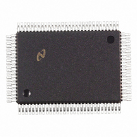
DP83902AVLJ National Semiconductor, DP83902AVLJ Datasheet - Page 50

DP83902AVLJ
Manufacturer Part Number
DP83902AVLJ
Description
IC CTRLR SER NETWORK IN 100PQFP
Manufacturer
National Semiconductor
Datasheet
1.DP83902AVJGNOPB.pdf
(70 pages)
Specifications of DP83902AVLJ
Controller Type
Serial Network Interface Controller
Interface
Serial
Voltage - Supply
4.75 V ~ 5.25 V
Current - Supply
140mA
Operating Temperature
0°C ~ 70°C
Mounting Type
Surface Mount
Package / Case
100-MQFP, 100-PQFP
Lead Free Status / RoHS Status
Contains lead / RoHS non-compliant
Other names
*DP83902AVLJ
Available stocks
Company
Part Number
Manufacturer
Quantity
Price
Company:
Part Number:
DP83902AVLJ
Manufacturer:
NS
Quantity:
2 500
Company:
Part Number:
DP83902AVLJ
Manufacturer:
RAYCHEM
Quantity:
2 500
Company:
Part Number:
DP83902AVLJ
Manufacturer:
Texas Instruments
Quantity:
10 000
Part Number:
DP83902AVLJ
Manufacturer:
NS/国半
Quantity:
20 000
14 0 Preliminary Electrical Characteristics
Absolute Maximum Ratings
If Military Aerospace specified devices are required
please contact the National Semiconductor Sales
Office Distributors for availability and specifications
Supply Voltage (V
DC Input Voltage (V
DC Output Voltage (V
Storage Temperature Range (T
Power Dissipation (PD)
Lead Temp (TL) (Soldering 10 sec )
ESD Rating (R
Pin to Pin
Pin to GND
Pin to V
Clamp Diode Current
Preliminary DC Specifications
Note 1 These levels are tested dynamically using a limited amount of functional test patterns please refer to AC test load
Note 2 Limited functional test patterns are performed at these input levels The majority of functional tests are performed at levels of 0V and 3V
Note 3 This is measured with a 0 1 F bypass capacitor between V
Note 4 The low drive CMOS compatible V
guaranteed by testing the high drive TTL compatible V
Note 5 RA0–RA3 PRD WACK BREQ and INT pins are used as outputs in test mode and as a result are tested as if they are TRI-STATE input outputs For these
pins the input leakage specification is I
Symbol
V
V
V
V
V
V
V
I
I
I
I
IN
INSEL
OZ
CC
OH
OL
IH
IH2
IL
IL2
LOL
CC
(
g
ZAP
1 ZAP)
Minimum High Level Output Voltage
(Notes 1 4)
Minimum Low Level Output Voltage
(Notes 1 4)
Minimum High Level Input Voltage (Note 2)
Minimum High Level Input Voltage
For RACK WACK (Note 2)
Maximum Low Level Input Voltage (Note 2)
Maximum Low Level Input Voltage
For RACK WACK (Note 2)
Good Link Output Voltage
Input Current
Input Current
Minimum TRI-STATE
Output Leakage Current (Note 5)
Average Supply Current
(Note 3)
CC
e
IN
)
OUT
)
1 5k C
)
ZAP
Parameter
OZ
STG
e
)
OH
100 pF)
b
b
and V
0 5V to V
0 5V to V
b
b
OL
OL
65 C to
0 5V to
limits are not tested directly Detailed device characterization validates that this specification can be
and V
CC
CC
OH
T
g
a
800 mW
A
a
a
a
20 mA
specification
1 5 kV
150 C
260 C
e
CC
7 0V
0 5V
0 5V
0 C to 70 C V
and GND
50
I
I
V
V
I
I
I
V
V
V
X1
I
OH
OH
OL
OL
OL
OUT
I
IN
IN
OUT
IN
which the safety of the device cannot be guaranteed They
are not meant to imply that the device should be operated at
these limits
mandatory isolation is employed and all differential signals
are taken to exist at the AUI or TPI side of the isolation
e
Note Absolute Maximum ratings are those values beyond
Note All specifications in this datasheet are valid only if the
e
e
e
e
e b
e b
e
e
e
Conditions
e
V
e
20 MHz Clock
CC
20 A
2 0 mA
16 mA
CC
V
GND
V
0 A
CC
CC
V
20 A
2 0 mA
e
or GND
CC
or GND
5V
or GND
g
5% unless otherwise specified
V
CC
b
b
Min
3 5
2 0
2 7
b
50
1 0
b
10
1
0 1
a
2000
Max
a
140
a
0 1
0 4
0 8
0 6
0 4
1 0
10
1
Units
mA
V
V
V
V
V
V
V
V
V
A
A
A
A


