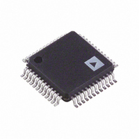
AD9953YSVZ Analog Devices Inc, AD9953YSVZ Datasheet - Page 21

AD9953YSVZ
Manufacturer Part Number
AD9953YSVZ
Description
IC DDS DAC 14BIT 400MSPS 48-TQFP
Manufacturer
Analog Devices Inc
Datasheet
1.AD9953YSVZ.pdf
(32 pages)
Specifications of AD9953YSVZ
Resolution (bits)
14 b
Master Fclk
400MHz
Tuning Word Width (bits)
32 b
Voltage - Supply
1.71 V ~ 1.96 V
Operating Temperature
-40°C ~ 105°C
Mounting Type
Surface Mount
Package / Case
48-TQFP Exposed Pad, 48-eTQFP, 48-HTQFP, 48-VQFP
Data Rate
25Mbps
Rf Ic Case Style
TQFP
No. Of Pins
48
Supply Voltage Range
1.71V To 1.89V, 3.135V To 3.465V
Operating Temperature Range
-40°C To +105°C
Msl
MSL 3 - 168 Hours
Frequency Max
400MHz
Lead Free Status / RoHS Status
Lead free / RoHS Compliant
For Use With
AD9953/PCB - BOARD EVAL FOR AD9953
Lead Free Status / RoHS Status
Lead free / RoHS Compliant, Lead free / RoHS Compliant
Available stocks
Company
Part Number
Manufacturer
Quantity
Price
Company:
Part Number:
AD9953YSVZ
Manufacturer:
Analog Devices Inc
Quantity:
135
Company:
Part Number:
AD9953YSVZ
Manufacturer:
ADI
Quantity:
329
Company:
Part Number:
AD9953YSVZ
Manufacturer:
Analog Devices Inc
Quantity:
10 000
Company:
Part Number:
AD9953YSVZ-REEL7
Manufacturer:
Analog Devices Inc
Quantity:
10 000
next address, and the timer reloads the ramp rate bits and
continues counting down. This sequence continues until the
RAM address generator has incremented to an address equal to
the RAM segment final address bits of the current RSCW. Upo
reaching this terminal address, the RAM address generator
reloads the RAM segment beginning address bits and the
sequence repeats.
The sequence of circulating through the speci
addresses repeats for as long as the part is programmed for th
mode. The no-dwell bit is a Don’t Care in this mode.
RAM Controlled Modes of Operation Notes and
Summary
Notes:
1.
2.
3.
The AD9953 offers five modes of RAM controlled operation
(see Table 6).
Table 6. RAM Modes of Operation
RSCW<7:5>
(Binary)
000
001
010
011
100
101, 110, 111
Internal Profile Control
The AD9953 offers a mode in which a composite frequency
sweep can be built, for which the timing control is software
programmable. The internal profile control capability disen-
gages the Profile<1:0> pins and enables the AD9953 to take
control of switching between profiles. Modes are defined that
allow continuous or single burst profile switches for three
combinations of profile selection bits. These are listed in
Table 7. When any of the CFR1<29:27> bits are active, the
internal profile control mode is engaged. Internal profile control
The user must ensure that the beginning address is lowe
than the final address.
Changing profiles or issuing an I/O UPDATE automatically
terminates the current sweep and starts the next sweep.
Setting the RAM destination bit true such that the RAM
output drives the phase offset adder is valid. While the
above discussion describes a frequency sweep, a phase
sweep operation is also available.
Mode
Direct Switch
Ramp Up
Bidirectional
Ramp
Continuous
Bidirectional
Ramp
Continuous
Recirculate
Open
Notes
No Sweeping, P
Valid, No Dwell Invalid
Sweeping, Profiles Valid,
No Dwell Valid
Sweeping, Profile <0>
Direction Control Bit, N
Dwell Invalid
Sweeping, Profiles V
No Dwell Invalid
Sweeping, Profiles Valid
No Dwell Invalid
Invalid Mode—Default To
Direct Switch
fied RAM
rofiles
alid,
Rev. A | Page 21 of 32
Is a
r
o
is
,
n
is only valid when the device is operating in RAM mode. T
is no internal profile control for linear sweeping operations.
When the internal profile control mode is engaged, the RAM
segment mode control bits are Don’t Care and the device
operates all profiles as if these mode control bits were
programmed for ramp-up mode. Switching between profile
occurs when the R
memory contents for the current profile.
Table 7. Internal Profile Control
CFR1<29:27>
(Binary)
000
001
010
011
100
101
110
111
A sin
exec
for ra
Logic 010(b). Upon receiving an I/O U
contr
mode sequence fo
final address value for Profile 0, the de
switch
sequence. Upon r
for P
begi
segment final
sequence is ov
Is
A continuous internal profile
composite sweep is continuously executed for as long as the
device is programmed into that mode. Using the example
above, except programming the CFR1<29:27> bits to Logic
101(b), the operation would be identical until the RAM
segment final address value for Profile 2 is reached. At this
point, instead of stopping the sequence, it repeats, starting with
Profile 0.
suing another I/O UPDATE restarts the burst process.
ns executing
uted once. Fo
rofile 1, the de
gle b
ol logic sign
mp-up mod
es to Profil
urst mo
add
er a
Mode Description
Internal Control Inactive
Internal Control Active, Single Burst, Activate
Profile 0, Then 1, Then Stop
Internal Control Active, Single Burst, Activate
Profile 0, Then 1, Then 2, Then Stop
Internal Control Active, Single Burst, Activa
Profile 0, Then 1, Then 2, Then 3, Then Stop
Internal Control Active, Continuous, Activate
Profile 0, Then 1, Then Loop Starting 0
Internal Control Active, Continuous, Activat
Profile 0, Then 1, Then 2
Internal Control Active, Continuous, Activate
Profile 0, Then 1, Then 2, Then 3, Then Loop
Starting 0
Invalid
e 1 and begin
als the device
that ramp-up
e and the C
eaching the RA
de is one in wh
r example, ass
ress va
nd the co
r Profil
AM address generator has exhausted the
vice automa
lue fo
e 0. Upon rea
mposite sw
FR1<29:2
control mode is one in which the
r Profile
s execu
to begi
tically sw
sequen
ume th
ich th
M se
ting that ramp-up
gment final addres
n executing the ramp-up
vice automatic
ce. When the RAM
ching the RAM segment
eep has completed.
e composite sweep is
7> bits are written to
e device is programme
2 is reached, the
PDATE, the int
, Then Loop Starting 0
itches to Profile 2 and
AD9953
ally
ernal
s value
here
te
s
e
d


